
High-Volume PCB Fabrication You Can Count On

Cost-effective. Scalable. Fully Certified.

As a trusted PCB fabrication manufacturer, Imagineering delivers production-grade printed circuit boards with zero compromises on quality or delivery.

Step 1

Design & Pre-Assembly Preparation

Every successful PCB assembly process starts long before a single component is placed. In this first stage, the focus is on preparing a design that’s not only functional but manufacturable. That means completing a full set of design files—schematics, Gerbers, BOM, and assembly drawings—and ensuring they align with Design for Manufacturability (DFM) principles.

What is a DFM Check?

A proper DFM check helps identify layout issues, spacing conflicts, or part selections that could complicate downstream processes.

This DFM process overview outlines what to look for.

What is a Bill of Materials?

Equally important is a clean, well-structured bill of materials. Procurement delays often stem from incomplete or outdated BOMs, so it’s worth double-checking part availability early.
This guide to PCB board design and layout walks through how to structure your files and layout for easier handoff.

Avoid Bottlenecks with Smart Design Choices

If you’re working on a tight timeline, small decisions now can have big downstream effects. For tips on avoiding bottlenecks, see our blog on speeding up the PCB assembly process. For more on simplifying handoffs and avoiding costly redesigns, talk to Imagineering. Our experts are ready to help you optimize your PCB layout before production begins.

What is a Solder Paste Application?

Solder paste is a grayish compound made of tiny solder particles suspended in flux. It’s applied through a laser-cut stencil that aligns with the board’s surface-mount pads. Each opening in the pencil allows paste to be deposited exactly where components will later be soldered.
This blog on the PCB assembly process walks through how stencil printing works in more detail.

Why is Precision So Important?

Even minor misalignments or inconsistent paste volumes can lead to defects like soldier bridges or cold joints. Modern assembly lines often use automated stencil printers to ensure consistency across runs.
To learn how solder defects can derail a project, check out our article on identifying and correcting solder bridge defects .
Step 2

Solder Paste Application

Once your design is locked in, it’s time to move from digital to physical. The first hands-on step in the PCB assembly process is applying solder paste—a critical step that sets the stage for accurate component placement and reliable solder joints.
Step 3

Component Placement

With solder paste applied, the board is ready for population. In this stage of the PCB assembly process, components are placed precisely onto the board’s surface-mount pads, with paste holding them in position before soldering.

What is Component Placement?

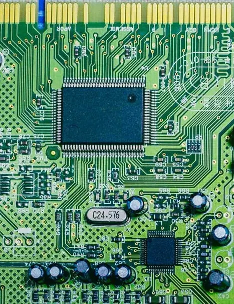
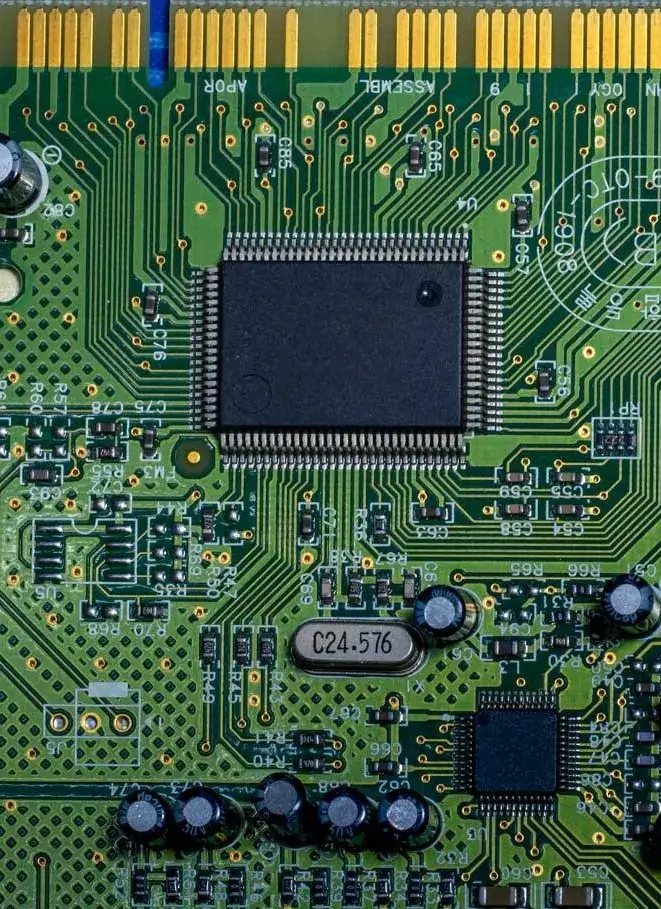
Most PCB assemblies today use automated pick-and-place machines that pull components from reels or trays and set them directly onto the board. These machines follow programmed coordinates derived from your design files, ensuring accuracy even at high speeds.

For a deeper look into how this works, explore our PCB assembly process overview.

What Technologies Are Involved?

Modern surface mount technology (SMT) has transformed this step. Machines can place thousands of parts per hour, including ultra- miniature chips, with precise orientation and spacing.Modern Surface Mount Technology (SMT) can place thousands of parts per hour with precise orientation and spacing.
If you’re considering SMT for your project, this post on the advantages of surface mount technology explains why it’s now the industry standard.
Step 4

Soldering Techniques

Once components are in place, the next step is to create permanent electrical and mechanical connections. Soldering is the technique of fusing component leads to PCB pads using heat and metal alloy.

Reflow Soldering (Surface-Mount Devices)

Most surface-mount assemblies go through a reflow oven. The board is heated in controlled stages until the solder paste melts, bonds, and then cools into solid joints. This is the most common technique for high- density SMT boards.

For a full walkthrough, see our PCB assembly process guide.

Through-Hole Soldering (Wave and Selective)

When through-hole parts are involved (like connectors or large components) wave soldering or selective soldering may be used. These methods handle the back side of the board or more complex mechanical parts.

For a deeper dive, visit our page on through-hole assembly tools and techniques.

High-Mix? High-Precision? No Problem.

Complex assemblies may require a combination of methods, sometimes with manual soldering for special parts.

You can learn more about our approach to precision work here: Precision PCB Assembly.

What is PCB Inspection?

Automated Optical Inspection (AOI) systems scan the board after soldering to flag missing components, alignment issues, or bad joints. These systems use high-resolution cameras and algorithms to spot inconsistencies faster and more accurately than manual checks

See our AOI process breakdown
for a closer look.

Advanced Techniques

For boards with hidden joints (like BGA packages), X-ray inspection is essential. This non-destructive method reveals internal defects that would otherwise go unnoticed.

To understand how inspection fits into the broader quality process, explore our guide to PCB inspection methods.

Ultimately, inspection is perhaps the most important aspect of the PCB assembly process. It not only ensures the final product works as intended, but can help by spotting issues early on in the production process and avoid slowdowns or recalls in the future.

Looking for zero-defect outcomes? Talk to Imagineering about integrating AOI, X-ray, and manual inspection into your next build..
Step 5

Component Placement

Soldering may complete the assembly, but quality assurance is what ensures reliability. Inspection catches defects in the PCB assembly process before the board ever reaches final testing.
Step 6

Testing Procedures

Inspection checks visual and mechanical accuracy, while testing confirms electrical performance. For example:

Test Type
What It Verifies
In-Circuit Testing (ICT)
Connectivity, values, polarity, shorts
Flying Probe
Great for low-volume builds, no custom fixture needed
Functional Testing

Power-up, signal behavior, real-world performance

In-Circuit and Functional Testing

In-Circuit testing uses probes or fixtures to validate individual nets and components. Once that passes, functional testing powers up the board to ensure it performs correctly under simulated conditions.

Our article on PCB testing fundamentals covers these steps in detail.

When Is Testing Critical?

In short: always. But especially for mission- critical or high-reliability applications like defense and aerospace.

Explore the most common PCB QA tests to learn what level of testing your PCB assembly process might require.
Reliable boards require reliable testing, which is why we place such a high priority on it. Make sure you’re choosing a PCB assembler that not only pays lip service to inspection and testing, but has the technology and expertise to match your performance goals.
Step 7

Final Assembly & Packaging

Once testing confirms functionality, the final touches of the PCB assembly process bring everything together for shipment or integration.

Cleaning and Post-Solder Work

Residual flux, solder balls, or surface contaminants are removed through ultrasonic or solvent cleaning. This is especially important when using water- soluble flux or building for sensitive applications. A properly cleaned board isn’t just prettier, but more reliable over time.

If through-hole components weren’t soldered earlier in the PCB assembly process, this is often when they’re manually installed or wave soldered.

Last Visual Checks

At the end of the PCB assembly process, a final inspection confirms no damage occurred during handling or cleaning. This includes verifying connector alignment, securing hardware like standoffs or heatsinks, and confirming label accuracy.

Packaging for Protection

Just before shipping, boards are sealed in anti-static bags, cushioned with ESD- safe foam, and boxed with care. In some cases, moisture- sensitive components may require vacuum sealing and desiccant packs.

For more on how we handle the final touches, explore our Turnkey PCB Assembly and Consignment Services.
Step 8

Advanced Considerations

For teams pushing the limits of performance, complexity, or reliability, certain strategies can make or break your build.

Design for Manufacturability (DFM)

Early collaboration with your assembly partner pays off. Minor layout changes like pad sizing, via placement, or fiducial alignment can dramatically improve yield and reduce costs.

For an example, see our overview on conformal coating and find out how post-assembly finishing can impact long-term durability.

Cutting-Edge Technologies

High-density interconnects, 0.3 mm pitch BGAs, and flexible hybrids require the right tooling and experience.

See how our precision PCB assembly capabilities support advanced builds across industries.

Complex Boards Deserve a Sophisticated Partner: Imagineering

The PCB assembly process is more than just a sequence of technical steps. It’s the foundation of product quality, performance, and reliability. From early design preparation to final testing and packaging, each phase plays a critical role in delivering a successful outcome.

If you want to work with a partner that understands the details, the deadlines, and the demands of real-world production, Imagineering is ready to help. With precision equipment, experienced engineers, and a commitment to quality, we’ll guide your project from concept to completion with confidence.

Contact Imagineering today to discuss your next PCB assembly project and see what’s possible when you get every step right.