
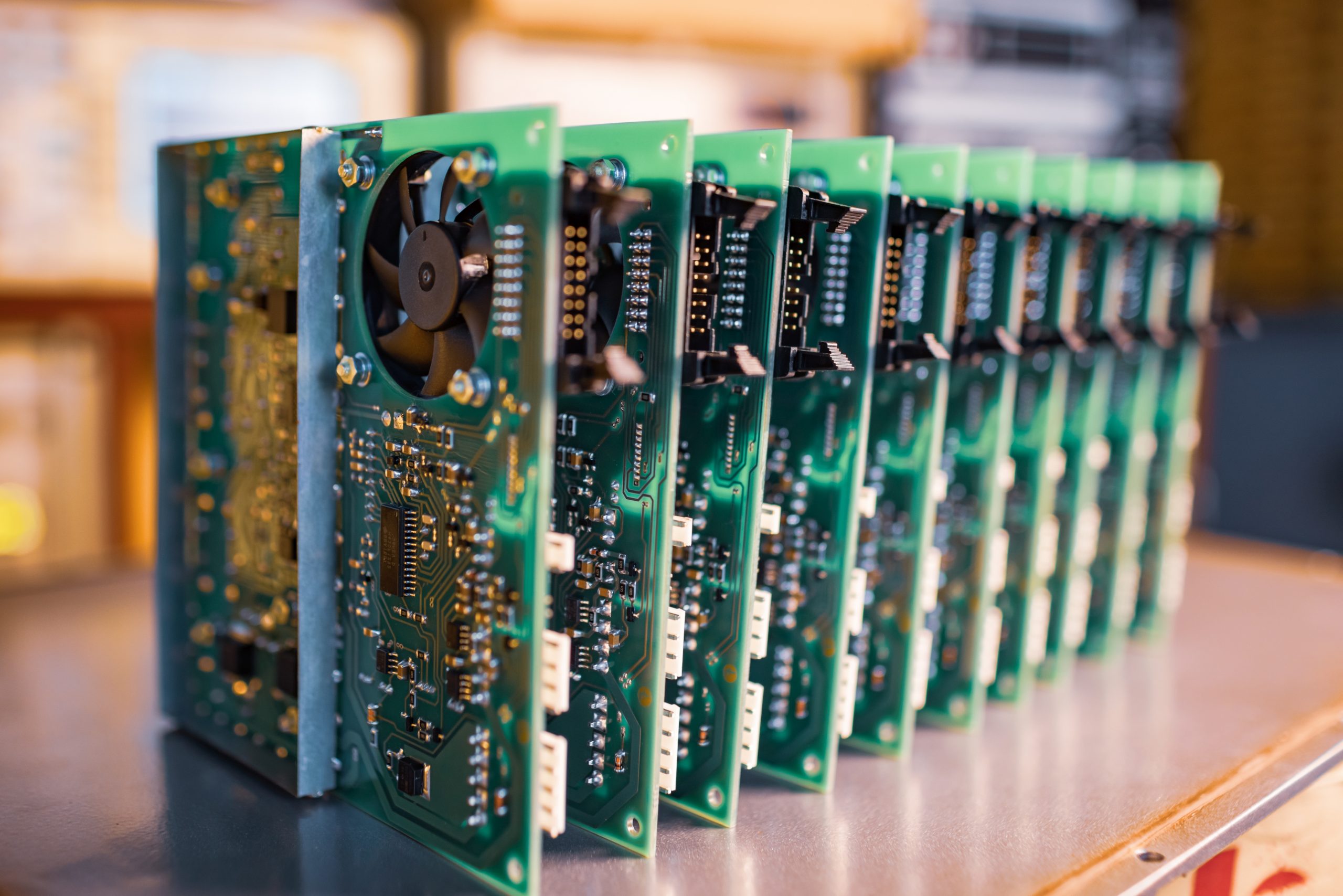
Without printed circuit boards (PCBs), the electronic devices that control, monitor, and regulate our daily lives in various environments would not exist. But, this miniaturization of electrical circuits has its challenges when it comes to the manufacturing and assembly of PCBs. Manufacturers must follow industry best practices to ensure these critical components do not fail, even as they speed up the PCB assembly process to meet ever-higher consumer demands.
There exists a close working relationship between PCB designers and manufacturers. Clear communication is one of the most critical drivers for a successful PCB prototyping stage. During this phase, design flaws can be identified, and best manufacturing practices are determined to fit the final product’s schedule, costs, and quality.
This partnership allows all stakeholders to work together as a team to create the desired PCB seamlessly. Read on for tips on creating a great relationship with your PCB maker.
Now, let’s dive into some tips for a successful PCB assembly!
PCB Assembly Tip 1: Plan your PCB Project Early
Optimizing PCB assembly requires careful planning, including a clear description of requirements such as the following:
- Bill of materials (BOM)
- Gerber files
- Pick and place file
- PCBA testing file
Additional information is often needed for the final PCB manufacture, including assembly drawings, 3D drawings, and schematics.
Manufacturers can prepare the fabrication and assembly phases more quickly with detailed documentation and PCB specifications and purchase the needed materials. It also allows them to improve the entire PCB design and assembly process while partnering with other key service providers, like PCB design software creator Altium Designer, which can help you get started with this process.
Maintaining clear lines of communication with your manufacturer helps ensure that your PCBs are only made with considering your needs. Choosing a manufacturer that matches your communication style and frequency helps ensure a smoother process.
Clear communications are especially important when the printed circuit board design is highly customized and features non-standard specifications. Experienced partners who follow best practices in PCB prototyping should also be able to offer important tips for PCB assembly, such as the latest techniques and best choice of materials. These benefits help minimize duplicate effort, so you don’t have to reinvent the wheel.
PCB Assembly Tip 2: Design for Manufacturability (DFM)
DFM is a general engineering practice for designing products to make them easy to manufacture. This process allows for easier detection of potential problems in the design phase, which is less expensive than discovering problems during manufacture. Edge clearance, acid traps, layout complexity, and solder masks between pads determine a PCB’s manufacturability.
While DFM is a common practice in virtually all engineering disciplines, the ways it is implemented can vary. For example, each PCB manufacturer uses its guidelines and procedures that can address possible production problems during the design phase.
These include consideration of the manufacturers’ capacity and capabilities, along with industry-wide best practices that are continually evolving. The trend towards greater automation in PCB assembly means design and manufacturing processes are generally becoming less costly. For example, using robotics for component placement and soldering of surface-mount technology (SMT) can significantly reduce the cost of PCB manufacturing.
DFM guidelines should include measures to avoid delays. This problem often occurs when you need additional interactions with the assembler to ensure the PCB’s manufacturability. The best approach is to work with the manufacturer early in the PCB prototyping phase so the PCBs are DFM-compliant from the beginning. Understanding the manufacturer’s DFM requirements is particularly important, allowing you to optimize the PCB design for efficient assembly.
Common factors to consider are circuit routing, panalization, and component placement. Minimize the use of complex or obsolete components that can slow down manufacturing and sourcing processes. Preliminary testing is a meaningful way to identify errors early in the design process and avoid the higher cost of fixing them during assembly, which requires rework.
DFM testing can detect problems with footprint corroboration, component spacing, and component polarity, provided it’s performed by experienced engineers specializing in these procedures. Specific benefits of DFM testing include reduced costs, improved product quality, and shorter delivery times.
Read: Design for Manufacturability (DFM) Process Overview
PCB Assembly Tip 3: Gain More Visibility into the Manufacturing Process
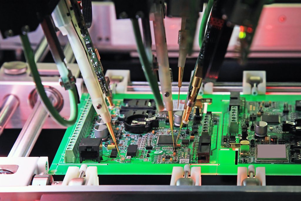
The quality of components used in the assembly of PCBs is crucial to the quality of the final product. A professional PCB assembler should have a quality assurance (QA) department that evaluates BOM components based on quality, date, and model number. In addition, assemblers should perform various tests on samples, such as material operational testing. A final inspection of PCB components should be performed to detect any missing or broken parts, circuit deformation, and oxidation.
Some PCB manufacturers allow their clients to make a site visit. If your manufacturer is one of them, you should conduct a visit as soon as possible to increase the visibility into the manufacturing process. For example, Imagineering has facilities in Elk Grove Village, Illinois, and Fort Worth, Texas.
Choosing the right PCB manufacturer can be particularly challenging in today’s global economy, largely due to the many choices available. However, finding one that offers clear communication, high-quality products, and fast turnaround times is essential. The United States (US) has some of the highest quality standards in the world, which are enforced by regulatory bodies like the International Organization for Standardization (ISO).
As a result, US-based PCB manufacturers must adhere to high standards that meet or exceed their customers’ expectations. Consider a manufacturer’s certifications when researching the best partner for your project. These manufacturers must also invest heavily in PCB prototyping to remain current on emerging technologies.
Get the design guide: A Guide to Design-for-Manufacturing (DFM) Principles.
PCB Assembly Tip 4: Align Expectations with the PCB Manufacturer
Collaboration between PCB designers and manufacturers can eliminate many challenges caused when the manufacturer needs to adequately understand the project’s requirements, specifications, or standards. This problem can result in discrepancies between the expected outcome and the final product.
Regular communication with your manufacturer makes it easier to address all stakeholders’ questions and concerns promptly. Your manufacturer should remain closely involved in the design review process, allowing them to provide insights and suggest improvement. In addition, you should offer feedback to your manufacturer after each production run, fostering a culture of continual improvement.
Collaboration is also important in PCB assembly because the engineers designing the schematic are rarely the ones assembling the PCB. Keep all team members in the loop when making design changes. Design teams often use exchange files to accomplish this goal, but other team members must identify themselves and the data they have changed.
This includes material suppliers that are directly connected to the manufacturer. Component procurement often has a lead time and can impact design changes involving new items. You may need to temporarily change materials during PCB prototyping as a test to see if it improves the final product in some way. Some collaboration tools for PCB designers include links to suppliers, providing real-time data on pricing and quantities.
PCB Assembly Tip 5: Clear and Detailed Documentation
Documenting a PCB design requires designers to clearly define their own work regions, meaning they need to mark out their space on the board. Work regions should remain uncluttered and easy to navigate, so designers can focus on their design rather than struggling with software to provide documentation. These tools should also allow designers to easily view the work of other designers on that board, so they can avoid conflicts or duplicated effort.
PCB Assembly Tip 6: Continuous Improvement and Feedback
The PCB assembly process can be improved by following the plan-do-check-act (PDCA) cycle. The Plan phase of this approach identifies opportunities for change and plans those changes. The Do phase implements changes on a small scale, while the Check phase analyzes the results to determine the effects of those changes. If the changes are beneficial, the Act phase implements them wider and continuously assesses the results.
Work with your PCB manufacturer to discover new opportunities for improvement, which is an essential component of DFM. This practice also requires you to collect and analyze data to identify areas to reduce scrap, promote assembly cycle times, and improve quality issues while reducing production bottlenecks.
Additional ways to optimize assembly include soliciting feedback from technicians, which you can then integrate into the current process. Regular review and refinement of the assembly process are vital for cultivating a continuous improvement mindset.
Strengthen Your PCB Assembly Process with Imagineering: Essential Strategies for Success
Many technological advances have improved the reliability and accuracy of PCB assembly, but the challenge is to make the process as seamless and efficient as possible. The best practices discussed above will help improve assembly, especially when combined with an experienced PCB manufacturer like Imagineering.
Implementing these tips will also increase the communication between PCB designers and manufacturers, which is critical to streamlining processes and optimizing the assembly workflow. These changes will ultimately accelerate PCB assembly and reduce time-to-market.

Stay up-to-date with our latest posts:
- What Is the PCB Fabrication Process? A Buyer’s Guide to Quality, Cost, and Manufacturability
- Understanding the PCB Fabrication Process: From Design to Delivery
- 5 PCB Prototyping Tips to Speed Up Your Development Cycle
- Circuit Board Repair: Common Reasons for PCB Failure (and How to Fix Them)
- A Guide to Printed Circuit Boards and Their Uses (2026 Edition)