Whether you're trying to get your latest product to market quickly, or just need a few boards to prototype your personal project, lmagineering is capable of producing industry-standard PCBs for any application.
We offer fully-certified, high-quality PCBs at any production volume you need, and we do it with a 100% on-time guarantee.
How do we do it? A combination of cutting-edge technology and decades of experience.
Manufacturing Capabilities
With production facilities at our Illinois headquarters and offshore facilities, we’re able to offer same-day prototypes and production in 5-7 days.
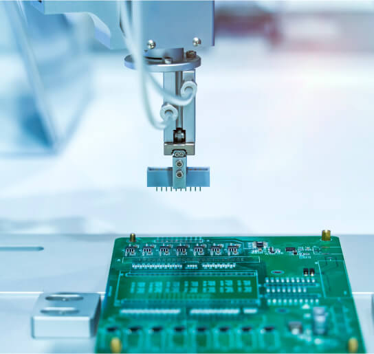
PCB Fabrication Services:
Items
Manufacturing Capabilities
Rigid & Flex PCBs
lmagineering offers multi-layer rigid and flex PCB fabrication.
High-Density Interconnect (HDI) Technology
We make the most of smaller components with our HDI technology.
Layer Count: Supports up to 50 layers.
Stacked Microvias: Expertise in microvia technology for complex, high-density designs.
Impedance Control: Precise impedance management for advanced electronic applications.
Materials and Thickness
We can produce PCBs with a minimum board thickness of 4 mil (0.004″) and a maximum thickness of 240 mil (0.240″).
Soldermask swell: Expansion over pad area is 0.004″ (0.002″ each side).
Copper Thickness
Up to 4 oz. copper thickness available.
Trace Width and Spacing:
0.5 oz. Copper: Minimum trace width/space 0.003″
1 oz. Copper: Minimum trace width/space 0.004″
2 oz. Copper: Minimum trace width/space 0.006″
3 oz. Copper: Minimum trace width/space 0.009″
4 oz. Copper: Minimum trace width/space 0.012″
PCB Assembly Services
Whether you’re sending us materials and build kits from your own supply chain, or relying on our full-service turnkey fabrication, we offer the following assembly services:
Surface mount technology (SMT)
Flipchip
Thru hole technology (THT)
Flex circuit assembly
Cable assemblies
PB-free assembly
Wire harness assembly
BGA, Micro-BGA, QFN and other leadless package parts
Design and Engineering Services
Design for Manufacturability (DFM) Checks
The first step in our production and manufacturing process is to ensure your design is optimized for performance and manufacturability. Learn more about our DFM checks.
Quality Assurance and Inspection
Items
Manufacturing Capabilities
Inspection Standards
Class II and Class Ill Inspection: We adhere to stringent industry standards for high-reliability applications.
Quality Assurance
X-Ray Inspection: Advanced X-ray technology for thorough inspection of hidden solder joints and internal structures.
Automated Optical Inspection: Precisely detects defects such as solder bridges, missing components, and misalignments.
Functionality Testing: We conduct comprehensive functionality tests, including electrical performance, signal integrity, and overall functionality to ensure that the final product meets all performance specifications and quality standards.
Fully Certified
Part of our dedication to quality is staying on top of all relevant industry standards.
We are:
IT AR Registered
An IPC Member
Compliant with RoHS
UL Approved
AS9100D/1SO9001:2015 Certified
SAM Registered
WEEE Certified
CCR Registered
ORCA Registered
Industries Served
For nearly 40 years, we’ve been focused on delivering high-quality, fully certified PCBs for customers in every industry. From hobbyist builders to international electronics manufacturers, we’ve experienced every roadblock and have the tools and experience needed to overcome them.
We’ve got firsthand knowledge in:
Medical Services
Defense
Consumer electronics
Aerospace
& many more.
If you’re unsure if we have the capabilities to produce what you need, get in touch with one of our experts and let’s see if we’re a good fit.
PCB Production and Support Excellence
Production Flexibility
Our international presence affords us access to economies of scale. That means we’re ready and willing to handle any volume of production you need. Whether you just need a prototype, or you’re looking for a full production run, we’re ready to help.
Facilities and Location
We have state of the art facilities located right here in the United States at our Elk Grove, IL headquarters. To support larger production runs, we also have offshore facilities.
On-Time Guarantee and Dedicated Support
100% On-Time Guarantee
We promise to meet any delivery schedule you need without compromise.
Customer Support
Our dedicated support team is ready to assist our clients throughout the project lifecycle.