In an age of smart devices and hyperconnectivity, nearly everything we use contains a printed circuit board. Printed circuit boards guide our lives as we turn on the car, text our friends, and turn on the television. Yet for an object that is nearly ubiquitous in our lifestyle, printed circuit boards remain nearly invisible for most people from day to day. The PCB assembly process brings life to these machines, turning plates into fully functioning computer brains that quietly operate around us.
The PCB assembly process differs from PCB fabrication. While PCB fabrication focuses on producing panels through laminating layers of fiberglass, epoxy, and copper, a PCB cannot function until component parts are attached to the surface. These parts range from resistors, transistors, capacitors, sensors, and other pieces that bring full functionality to an end product.
What does the PCB assembly process look like? In this blog, we examine each stage of the process below.
The Stages of the Printed Circuit Board Assembly Process
Pre-Production
Before the printed circuit board assembly process can begin, a design file is generally reviewed for potential errors so they can be resolved. A design for manufacturability check, or DFM check, is a design analysis that is performed prior to production to ensure that any issues are resolved well in advance. This is performed to determine if any of the features in the design will be problematic during the production process.
For instance, with the push towards miniaturization, spacing between components can often be too small, leading to short and malfunctioning parts. A DFM check can prevent these issues from becoming a problem during the production process, preventing the waste of boards that don’t function properly. Redundancies and missing parts can also be addressed to cut costs.
Solder Paste Printing
The first step in the printed circuit board assembly process is solder paste jet printing. Solder paste is a material that contains small balls of metal (solder) with a specialized chemical that helps them bind to the surface of the printed circuit board when heated up.
A solder paste jet printer disperses the fluid at 300 dots per second. This method allows extreme precision and no wasted material, allowing for rapid board revisions and eliminating board transfer time.
After application, solder paste will only remain on the places where components will be attached. A machine will then perform an inspection to ensure that solder paste was evenly applied to the PCB. What remains is referred to as a prepared printed circuit board.
Pick and Place
With solder attached to predetermined areas of the prepared PCB, it is then conveyed to a pick and place machine. A robotic hand is able to precisely move surface mount components onto the printed circuit board. These machines can swiftly attach surface mount components into their precise locations. At this stage, the solder paste and components are connected, but are unfused.
Reflow Soldering
With the surface mount components placed on the printed circuit board, the solder now must be heated up to fuse them together. The printed circuit board is moved via conveyor belt into a “reflow oven” that melts the solder paste. The process functions similarly to a pizza oven, carefully applying the correct amount of heat for a precise period of time.
For two-sided PCB assembly, both sides will require separate stenciling and reflowing.
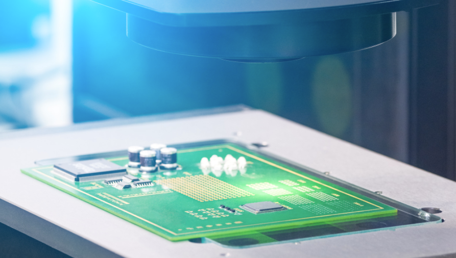
Inspection
At this stage of the PCB assembly process, the majority of installation work has been completed. However, inspection and quality control are essential, as reflow can sometimes lead to movement on the board that can cause shorts or faulty connections.
Manual inspection may be used for smaller batches of PCBs, but the inspection process has largely been automated. Solder connections can reflect differently depending on the quality of the connection, and machines have been programmed to recognize faulty connections at a rapid pace. X-rays may also be used for multi-layer PCBs.
After the inspection process, the printed circuit board is tested to ensure it can function properly. This final test for functionality simulates normal activity a printed circuit board will go through during its life cycle. If voltage, current, or signal output are above the acceptable range, they will be recycled or scrapped.
For every PCB assembly job, testing must occur on an ongoing basis to ensure that the quality of the boards remain static throughout a production cycle. Class 3 printed circuit boards generally have stricter requirements around testing, raising the time and cost of the assembly process.
Get a PCB Assembly Quote Today with Imagineering
With so many moving parts, it is critical that you have a printed circuit board manufacturing partner that not only understands how the printed circuit board process works, but how it can be produced at the best quality and lowest cost.
Imagineering Inc is a proven PCB assembly manufacturer headquartered in the USA. We excel at quick turnarounds at aerospace quality, providing the best service for manufacturers across all industries.
Get a quote on PCB assembly today.