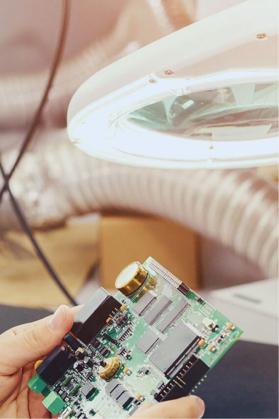
Our PCB fabrication tolerances ensure your boards are built to spec, reliable in performance, and production-ready from day one.
Getting It Right the First Time
When it comes to PCBs, precision is the foundation of performance. Every trace width, drill hole, and copper-to-edge clearance falls under the banner of tolerance in manufacturing. Even the smallest deviation can cause delays, assembly headaches, or outright failure.
Here’s what tight tolerances mean for your project:
Boards that meet spec and function as intended, without costly rework.
Proper hole alignment and registration mean smoother downstream builds.
Push density and complexity, knowing your boards can be manufactured.
At Imagineering, our tolerance standards are engineered to eliminate surprises so your designs work right, the first time.
Built Per Your Specs
Our boards are manufactured to exacting standards so your designs scale smoothly from prototype to production. Here’s what you can expect:
Quality & Certifications You Can Trust
When you partner with Imagineering, you’re getting more than specs on a page. We show our commitment through actions, not words. Our proof is certified adherence to internationally recognized standards and decades of consistent delivery.
Experience. Reliability. Results.
When tolerance in manufacturing is critical, you need a partner who delivers more than numbers on a chart. Here’s what sets Imagineering apart:
37+ years of expertise in precision PCB fabrication and assembly
30,000+ customers served across aerospace, medical, defense, and consumer markets
Prototype-to-production consistency with no vendor handoffs
Award-winning on-time delivery – Service Excellence Award 2023
Certified to AS9100D, ISO 9001:2015, ITAR, UL, and RoHS
Every board we build is backed by the same commitment to accuracy and dependability that has defined us since 1986.
Trusted Where Precision Matters Most
Our fabrication tolerances are proven in environments where failure is not an option. Imagineering builds boards for industries that demand absolute accuracy and reliability:
Mission-critical systems with zero margin for error
life-saving technologies built on precise, dependable PCBs
high-speed, compact designs that power innovation on the road and in connected devices
robust boards that perform reliably in demanding applications
Tolerance in Manufacturing, Without Compromise
When it comes to tolerance in manufacturing, Imagineering delivers confidence.
Every board is built to exacting standards, verified by certified processes, and backed by decades of experience serving industries where precision is everything.
From first prototypes to production-scale runs, you can trust Imagineering to keep your project on schedule, on spec, and ready for what’s next.
HQ
1389 Brumlow Ave
Southlake, TX 76092
PCB Assembly
2425 Touhy Ave
Elk Grove Village, IL 60007
Phone:(847)806-0003
Email:Sales@PCBnet.com
ITAR Registered
AS9100D/ISO9001:2015
SAM Registered
RoHS Compliant
Copyright © 2023 Imagineering, Inc Web Design by Solid Digital
