Have you ever wondered why printed circuit boards (PCB) are always green?
It’s the solder! During the PCB assembly process, the solder mask stays behind, making the circuit board appear green.
Today’s assembly of PCBs has come a long way, and if you positively want to know more about it, you’re in the right place.
Keep reading while we take a look at how the process of manufacturing PCB uses today’s tech.
What Is a Printed Circuit Board?
If you haven’t heard of PCBs, you’ve probably used the devices they come in, like computers and cell phones, to name a couple. They are the unsung heroes of electronic devices.
What are they? The components of electronic devices need a way to communicate; PCBs are the backbone that provides it.
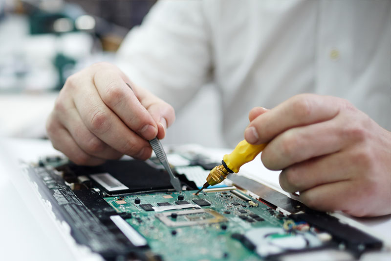
If you’ve ever disassembled a cellphone, broken a TV remote, or taken apart a computer for any reason, you would have seen a green-looking circuit board inside. That’s a PCB.
How Does PCB Assembly Work?
The process of PCB assembly has several separate steps. The very first is choosing the best base for your framework. Copper is the most prevalent metal base that most experts say safely conducts electricity and doesn’t heat itself.
Once the base is set, you move on to the other steps. These include:
Applying the Solder Paste
This step begins after the PCB is prepared and ready. This solder is the binding between the electronic components and the PCB. Experts say this is the most critical step in the surface mount assembly process.
The correct amount of paste must be applied to each pad being soldered to the PCB. Not doing this step correctly can result in a defective PCB. Experts recommend using certified designers and manufacturers to avoid high failure rates.
The Component Placement
It is necessary to place the components after applying the solder paste. This step uses Surface Mount Technology (SMT), where the components are affixed precisely onto the PCB. Using SMT comes with some benefits.
For example, components can be placed closer together, making the final PCB product smaller and more lightweight. Maintaining this level of precision is nearly impossible when affixing the components by hand. For this reason, most manufacturers use pick-and-place machines for better results.
The information about where the components are required to be placed are given in the PCB design. These details make it programming the pick-and-place machine a straightforward process.
The Reflow Oven
After the components are all in place, the PCB is moved to the conveyor belt for the reflow oven. This step is where the actual connection will take place. The solder that was applied during the solder paste step now will melt during the reflow soldering step, and this joins the components to the PCB permanently.
The Cleaning of the PCB
After the soldering of the PCB, cleaning is a critical step. It can affect the overall durability, effectiveness, reliability, and lifetime of a device. Throughout the assembly process, the PCB can become soiled with solder or flux, dirt from handling, or the environment, like residues, moisture, dust, colophony or resin, fingerprints, or oxides.
What’s more, some contaminants can have erosive effects that can damage the PCBs’ circuits and connections in the future, causing shorter lifespans, shorts, or failures in the device. The best way to ensure this doesn’t happen is to clean away all types of debris from the PCB.
When cleaning the PCB assemblies, your primary concern should be to remove any remaining resin and flux deposits from populated PCBs. It helps to have a clean and clear PCB when you are ready to inspect the board.
The PCB Assembly Inspection
Naturally, the inspection of the PCB is a critical step. Given the complexity of these devices and the need to ensure their reliability, many PCB manufacturers are now using advanced inspection techniques.
In automatic inspections, the primary technologies used are optical inspection, X-ray inspection, laser triangle measurement, and X-ray lamination technology. During this inspection step, you are checking the PCB for loose solder balls, shorts, or bridges between solder balls.
The Final Step in the PCB Assembly Process
Testing PCBs at various stages throughout the assembly process is essential to avoid situations where defects are found at the last moment. For example, when the boards have already gone into production or are in the market.
No matter how diligent the designers and manufacturers are, there is a risk that defects, human errors, or bugs will occur at any point.
What should you test? As PCBs have a few different parts, each impacting the overall circuit and electronics assembly. Therefore, it would be ideal for testing everything. Some things to include are:
- Mechanical strength
- Electrical conduction
- Purity
- Soldering quality
- Lamination – Peel and strength
- Hole wall quality
- Component polarity, placement, alignment, positioning, etc.
Testing primarily involves monitoring the product that will deliver the sought output. Several methods are used to ascertain this, and where there are failures, they are analyzed to determine where the faults occurred.
What’s Next for the PCB Assembly?
This brings us to the end of the PCB assembly line. If you want your PBC to work the way you planned it, it’s best to hire certified and experienced people. Another way to get it done is to farm the work out to accredited firms. Many firms can help design and produce a PCB in the US during these challenging times that do everything you need at a reasonable price. Imagineering has experts waiting to consult. Get in touch to find out more.