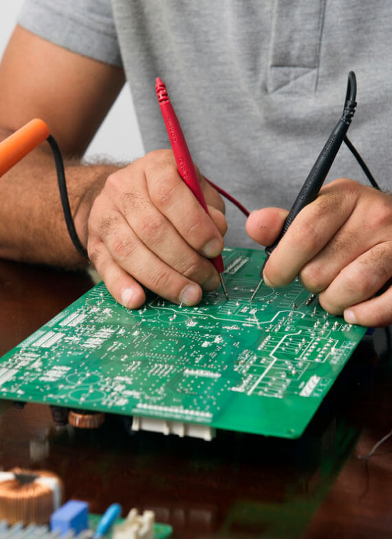
Smaller, faster, more reliable designs built with Imagineering’s proven expertise.
Everything we do at Imagineering boils down to one question: how can we help innovators push the limits of design?
For us, high density interconnect (HDI) represents the culmination of that work.
With over 37 years of experience, AS9100D/ISO-certified processes, and award-winning on-time delivery, we’re trusted by engineers in aerospace, medical, industrial, and consumer electronics.
From the first prototype to full production, our team builds HDI boards with the same precision and dependability we’ve delivered to more than 30,000 customers worldwide.
Why HDI Matters
High density interconnect PCBs let you do more with less. Less space, less weight, and less signal loss. For engineers working on cutting-edge applications, that means faster performance and more reliable designs in smaller packages.
What We Can Build
Engineers choose Imagineering for high density interconnect PCBs because our capabilities match the toughest design challenges. Whether you’re routing fine-pitch BGAs or stacking multiple sequential laminations, we deliver the precision needed to keep your project on track.
Stronger Vias. Smarter Process.
Not all HDI builds are created equal. At Imagineering, we use a plate-shut via fill process instead of standard non-conductive resin fills. The result is microvias that are fully metallic, structurally robust, and electrically reliable.
Every HDI board we ship is backed by our certifications:
When your design demands uncompromising reliability, our process and certifications ensure it performs as intended every time.
From bare board to finished build–all under one roof.
HDI designs don’t have time for vendor handoffs. At Imagineering, we handle both fabrication and assembly in-house, so you can go from CAD file to a fully assembled board without juggling multiple suppliers.
The Imagineering Advantage:
One partner from start to finish
Trusted where performance matters most.
Our high density interconnect PCBs power designs across industries where failure isn’t an option:
mission-critical systems built for reliability
precision boards for life-saving technologies
compact designs without compromise
high-speed performance in small form factors
Experience. Reliability. Results.
When it comes to high density interconnect PCBs, you need a partner you can trust. Here’s what sets us apart:
High density interconnect PCBs are the backbone of today’s most advanced electronics. Imagineering builds them with the precision, reliability, and speed your projects demand.
Imagineering builds them with the precision, reliability, and speed your projects demand.
From first prototypes to production-ready runs, we’re here to help you shrink designs, boost performance, and hit your deadlines.
HQ
1389 Brumlow Ave
Southlake, TX 76092
PCB Assembly
2425 Touhy Ave
Elk Grove Village, IL 60007
Phone:(847)806-0003
Email:Sales@PCBnet.com
ITAR Registered
AS9100D/ISO9001:2015
SAM Registered
RoHS Compliant
Copyright © 2023 Imagineering, Inc Web Design by Solid Digital
