PCB fabrication is the process of creating bare boards that will serve as the foundation for printed circuit board assembly.
You should choose your PCB fabrication contractor with care, as even small errors can damage the entire board, rendering the end product useless. Communication between the design team and manufacturers is critical, especially as manufacturing has moved overseas.
In this post, we explore everything you need to know about the PCB fabrication process, including the pre-process, PCB fabrication in full, and considerations to make when choosing a PCB fabrication company.
What is the Difference Between PCB Fabrication and PCB Assembly Process?
PCB fabrication and PCB assembly are two distinct parts of the PCB manufacturing process.
PCB fabrication is the process of transcribing a circuit board design onto the physical structure of the board. By contrast, PCB assembly is the process of actually placing components onto the board to make it functional. PCB fabrication can be likened to the paths, streets, and zoning of a city, while PCB assembly is the actual building that allows a printed circuit board to operate. More on PCB assembly can be found here.
Steps Before Starting the PCB Fabrication Process
Fabricating a printed circuit board is all about details. The initial design needs to be completed, as even a single component update that hasn’t been synchronized can lead to a bad board build. This includes:
- A complete engineering review for circuitry
- Synchronized schematic and layout databases
- Complete circuit simulation, signal integrity, and power integrity analysis
- Checked PCB design rules and constraints
- Bill of materials and design for manufacturing rules are reviewed
Read our Guide to Design-for-Manufacturing (DFM) Principals
The PCB Fabrication Process
Laser Direct Imaging and Develop/Etch/Strip Process
Before PCB fabrication can begin, laser direct imaging (LDI) is used to apply areas that will becomes the traces, pads, and metal ground of a printed circuit board.
- A dry film is applied to a copper laminate.
- Laser direct imaging exposes certain parts of the board to light in the shape of the PCB pattern.
- Any unexposed parts of the board will develop off, leaving the remaining film as an etch barrier
- The remaining film serves as an etch barrier that will be removed from the exposed copper to form the copper circuitry.
After this, an automated optical inspection inspects the layers for defects before they are laminated together. Any errors, such as potential shorts or opens, can be corrected at this stage.
Oxide and Lamination
With all of the layers etched, a chemical treatment called oxide is applied to the inner layers of a printed circuit board to improve the strength of the bond. Then, alternating layers of prepreg and copper foil are laminated together with heat and a hydraulic press. Prepreg is a fiberglass material containing an epoxy resin that melts from the heat and pressure of lamination, bonding the layers into a “PCB sandwich”.
Careful attention is required to ensure that alignment of circuitry between each layer is maintained.
Drilling
In order for a multi-layer printed circuit board to send signals from one layer to another, holes must be drilled or lasered in to form vias which connect them. Drilling differs depending on the type of via being used, but generally is done on a stack of 2-3 panels at a time. The end result will generally be 5 mil larger than the end product, as these holes will be plated with copper to help send electrical signals through a process called electroless copper deposition.
Blind and buried vias must be fabricated before the lamination process. Including these into your PCB design can increase the cost due to extra steps that must be taken.
Electroless Copper Deposition & Dry Film Outer Layer
After holes are drilled into the surface, excess resin and debris are cleaned using chemical and mechanical processes. Once removed, a thin coating of copper is deposited on all exposed parts of a panel, creating a metallic base for the electroplating process. Similar to the develop/etch/strip process from before, dry film is applied to the outer layers of the copper panel and is exposed to laser direct imaging, leaving a conductive pattern.
Electroplating, Stripping, and Etching
With the conductive pattern and drilled holes exposed, the panel is placed into a copper plating bath containing sulfuric acid and copper sulfate. When an electrical current is added into this, copper is deposited onto the conductive surface of the board with a thickness of about 1 mil. The plate is then removed and placed into a tin plating bath to serve as an etch barrier.
As plating is completed, the dry film is removed and the exposed copper not cover by tin is etched away, leaving only the traces, pads, and other patterns on the plate. The remaining tin is then chemically stripped, leaving only copper in precise areas.
At this point, the printed circuit board is now assembled – but it isn’t quite ready for assembly.
Solder Mask, Silkscreen, and Surface Finish
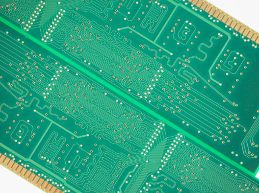
Before moving to the PCB assembly stage, the printed circuit board will be protected with a solder mask using a similar UV exposure found in the photoresist stage. This gives printed circuit board its distinctive green color, although other options are available.
A solder mask is a thin layer of polymer that protects the copper traces that have been printed onto the board from oxidation. It also prevents solder bridges – when unintentional connects form between two conductors, rendering the functionality of a printed circuit board.
Solder mask color can be chosen at this stage, but generally manufacturers use green, as it helps for defect inspection thanks to its high contrast and trace visibility critical to the PCB prototyping stage. Solder mask color doesn’t generally affect the functionality of a board, although darker colors are more heat-absorbent, making them impractical for high-temperature applications.
Once the solder mask has been applied, component reference designators and additional board markings are silkscreened onto the printed circuit board. The solder mask and silkscreened ink are cured by baking the circuit board in an oven.
Finally, a surface finish is applied to exposed metal surfaces not covered by the solder mask. This protects the metal and helps with soldering during the PCB assembly process.
Assembly Preparation, Inspection, and Testing
With the PCB fabrication process now complete, the finished boards undergo a series of inspections and tests to ensure their functionality before assembly or shipping. Automated test equipment seeks any shorts that can compromise the functionality of a board, and any PCBs that fail to meet the test are discarded.
Considerations for the PCB Fabrication Process
PCB fabrication is a detail-intensive process, and even simple mistakes can cost businesses through faulty construction. When choosing your PCB fabrication company, consider using PCB fabricators with a demonstrated record of success. Imagineering Inc produces aerospace-quality PCBs and can handle both the PCB fabrication and assembly processes. Our qualifications include the following:
- Turnaround in as little as 24 hours
- High mix low-to-mid volume
- Class II and Class III inspection
- AS9100D certified and ITAR compliant
- Leaded and lead-free RoHS assembly
- 100% on-time guarantee
- Design services (Outsourced)
- Full box build
If you’re looking for the best quality PCB fabrication company, look no further than Imagineering Inc. Our pricing is competitive, and our speed can’t be beaten. Get a quote for PCB fabrication now.