
The miniaturization of integrated circuits led to a revolution in smaller and more compact product design: HDI microvias are now an essential component in everything from aerospace PCBs to the chip in your phone. High Density Interconnection PCB design has gotten considerably more advanced over time – with better tools able to create smaller circuit boards, consumers can enjoy greater efficiency in smaller packages.
The ability to create smaller circuit boards would not be possible without the microvia. What are HDI microvias, and how do they contribute to better PCB design? In this blog, we explore how microvias play into the larger picture of circuit board manufacturing, and the benefits of implementing them into your PCB design process.
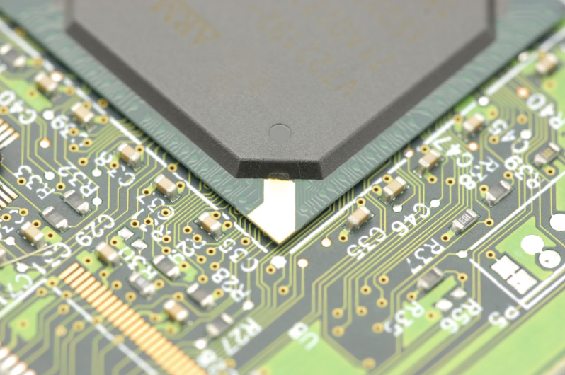
What Are Vias in a Printed Circuit Board?
Most printed circuit boards on the market today are built with several dielectric layers, surfaces that are polarized so that electricity doesn’t accidentally transfer from one layer to another. Layering allows for more information to be compressed into a single PCB. However, in order for a printed circuit board to function properly, electrical signals need specific entry points so that signals can pass through layers as needed. To connect from one layer to another, vias are perforated into the surface.
Printed circuit boards are often compared to buildings or cities to explain their functionality. A PCB via acts a bit like an elevator, passing signals from one floor to the next. They can be drilled or laser cut into a surface of a layer. Vias function as conductive pathways that come in a variety of formats.
- Through hole vias – A hole connecting from the top layer to the bottom layer of a printed circuit board, connecting both without interference from other layers of a PCB.
- Blind vias – A hole that connects from either the top or bottom layer to an interior layer. Once the printed circuit board has been laminated, the other end of the hole is invisible, hence the name “blind vias”.
- Buried vias – A hole layered between the top and bottom of a printed circuit board that connects multiple parts of a printed circuit board. Because they are not visible without a cross section of a PCB, they are also known as hidden vias.
What all of these vias have in common is their aspect ratio, a number that determines the reliability of a printed circuit board. This is calculated by dividing the thickness of a printed circuit board by the diameter of a drilled hole. The larger this ratio is, the lower their reliability.
Why is this the case? Once a hole has been made in the surface of a printed circuit board, it needs to be covered with a layer of copper plating. A larger aspect ratio can lead to non-uniform copper plating, decreasing the reliability of the end product. Additionally, larger holes are often mechanically drilled, leaving residue in its wake that can contribute to manufacturing defects.
Blind and buried vias tend to take up less space on a printed circuit board to allow for a fine I/O pitch. As a result, engineers have spent the past two decades refining the process to make these vias as small as possible, with the objective of using smaller die pads, including more chips in less space, and improving electrical performance.
Out of the need for smaller vias, microvias were born, and now represent the cutting edge of HDI PCB design.
What Are Microvias?
A microvia is the smallest via available in PCB assembly. ICP standards define a microvia as a hole with an aspect ratio of 1:1, with a hole diameter of 150 microns or less, and usually only connects one layer of a board to an adjacent layer. Microvias can be formed by photolithography, photodefining dielectrics, reactive ion etching, and laser ablation.
The rise of handheld electronic devices has sparked technological innovation in this field. Microvias are popular because they can provide for increased density on a smaller substrate, allowing for more portability in devices ranging from laptop computers, tablets, smartphones, and more. The need for smaller technology has also changed the way that they are layered on top of one another – while microvias tend to only connect adjacent layers, they can be arranged in a manner such that they allow for information to pass through multiple layers of a circuit board. These are referred to as stacked and staggered microvias.
- Stacked Microvias – Stacked microvias are when a series of microvias is placed on top of each other in a straight chain.
- Staggered Microvias – Rather than being aligned in a straight line, staggered microvias are arranged in a cascade moving down several layers. If a stacked microvias looks like an elevator shaft, staggered microvias resemble something closer to a stairwell.
Both of these methods are efficient methods of building vias between multiple layers. However, stacked microvias tend to be more expensive and time consuming to manufacture, as the stacked vias need to be filled and planarized.
Why Use HDI Microvias?
Microvias are implemented in high-density interconnect (HDI) layers, printed circuit boards with a higher wiring density than traditional PCBs. Per a study published by MIT, an HDI is made of a number of layers of conducting materials, consisting of the signal, power, and ground connections, which are then separated by dielectric material, glued together by an adhesive, and linked together by microvias. Leveraging HDI microvias boasts a vast array of benefits to those using them, including:
- Compactness – HDI PCBs have a much higher wiring capacity, making them the best option available for a small circuit board boasting tremendous output. HDI PCBs can dramatically lower the number of layers needed to function. For products that rely on small design constraints, these printed circuit boards are a necessity.
- Higher Heat Resistance – Because HDI microvias are made using the smallest holes possible with laser drill technology, the board as a whole has higher heat resistance.
- Faster Signal Transmission – HDI PCBs use space with much greater efficiency than their counterparts, meaning more circuitry can be placed on a single surface. With less distance to travel, electrical signals lead to increased performance and functionality by producing additional input and output, resulting a sharp decline in signal loss and crossing delays.
- Quicker Prototyping – HDI design diminishes the time and money put into designing and implementing prototypes. With shorter lead times, profit margins increase in turn.
- Lower Materials Cost – HDI PCBs use significantly less material than comparable circuit boards for increased performance power. This efficiency directly translates into less materials used during the production process, allowing you to generate higher volumes of revenue.
In short, HDI printed circuit boards have better performance, are more cost effective, and lead to higher volumes of revenue over time. With a smaller design, these circuit boards allow for a larger variety of applications across the board, from aeronautics to consumer products.
How HDI Microvias are Used in Product Design
Microvias solve a major problem in printed circuit board design: accommodating as much as possible into a limited amount of “real estate” on layers of a printed circuit board. In the process, microvias have not only allowed for the functionality of a computer to fit in our pockets, but has led to decreased costs for consumers as well as greater reliability and efficiency for the products themselves.
Every year, printed circuit boards grow smaller and smaller while engineers work to make them perform at higher clock rates. PCB fabrication houses must contend with the challenges that come with miniaturization standards that change on a yearly basis. For this reason, finding a reliable fabrication partner has never been more important than now.
Imagineering Inc. specializes in providing the highest quality with certifications that match your business. Whether you need a simple prototype or a complex multilayer or complete production run, Imagineering gets the job done on your timeline. Contact us today for more information about our services.