
Your phone wakes you up, your toaster makes you breakfast, your electronic vehicle gets you to work, and every one of these technologies relies on a printed circuit board, also known as a PCB.
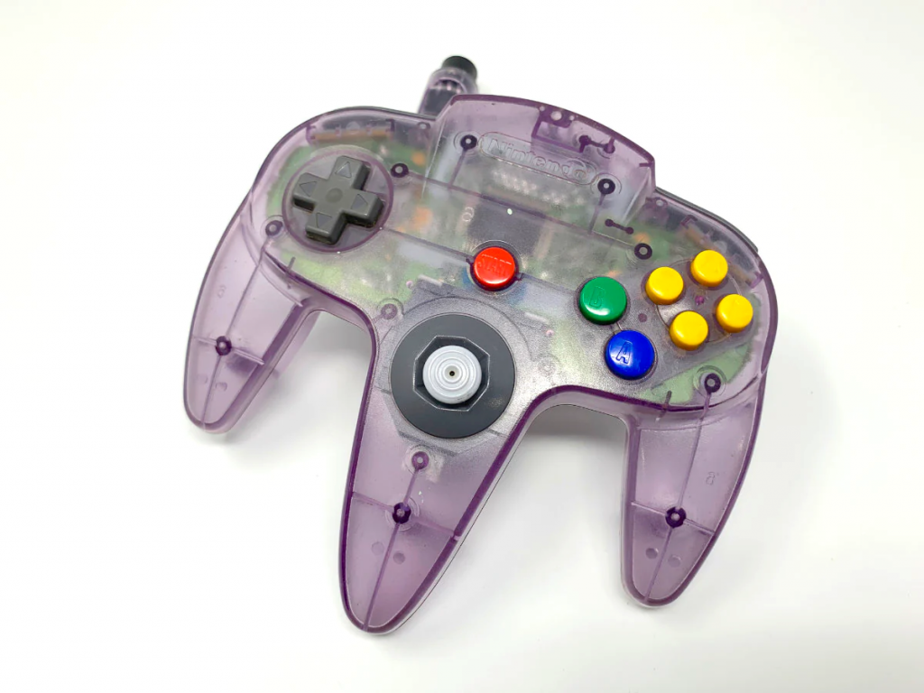
You’ve undoubtedly seen them before: green, flat boards with complicated-looking circuitry adorning their surfaces. If you’ve ever wondered about the creation process behind these modern marvels you see on your computer, your tablet, and, of course, inside that clear Nintendo-64 controller from your childhood, you’ve come to the right place.
Today’s blog will explain the PCB manufacturing process, from design to quality control, so you can better understand the boards that help our modern world turn.
Understanding Printed Circuit Board Basics
PCBs are flat, rigid boards made from non-conductive materials like fiberglass. They are etched with copper pathways along their surfaces, which serve as connections between various electronic components within a device.
PCBs can be thought of as the structural foundation of most modern electronic devices. Their purpose as a platform for mounting and interconnecting components makes them an invaluable tool for technology developers in almost every major industry, including aerospace, automobiles, and consumer electronics.
In a production process where even slight deviations can lead to malfunctioning devices, manufacturers have had to develop some ingenious solutions and tools to ensure consistent, high-quality outputs for their customers.
Basic Printed Circuit Board Components
Since printed circuit boards are used in most electronic devices, their designs vary widely. However, they generally share a few key characteristics.
- Substrate: This is the base material of the PCB. Most commonly, this is fiberglass-reinforced epoxy or FR-4.
- Copper Layers: Copper is used to create conductive pathways on the PCB.
- Solder Mask: This is a protective layer, typically made of epoxy resin. It’s applied to certain board areas to protect them from the soldering process.
- Silkscreen: This printed layer contains labels, symbols, and markings for components.
- Vias: Small holes drilled through the PCB, often plated with copper.
- Pads: Areas of exposed copper on the PCB. They provide a stable and conductive surface for solder joints.
PCB Design Phase
PCBs are usually designed by companies that create electronic devices and assembled by dedicated PCB manufacturers like Imagineering. Here’s an overview of that design process.
Step 1: Schematic Design
Engineers will design schematics that define the purpose of the PCB. These schematics will include required components, specifications, and connections.
Although the schematic will include a general board layout, the critical task of finalizing the layout is a separate step.
Step 2: PCB Layout Design
Once the schematic has been designed, it needs to be translated into a physical layout.
This is more complicated than it sounds—it means carefully considering many intricate factors like signal integrity, power distribution, and thermal management.
Ultimately, the layout design will include information like how to route the traces, the component footprints, placements of layers, and vias.
The layout design is a critical step in confirming the manufacturability of the PCB and is typically guided by the rules and constraints set by the PCB manufacturer. While this step can be complicated, PCB software programs can assist with this step. The biggest reasons for using PCB design software include improved efficiency, increased precision, and cost savings.
Step 3: PCB Manufacturing Process
Once designs are finalized, the manufacturing process can begin by choosing an appropriate substrate material.
I. Substrate Material Selection
Common PCB board materials include:
- FR-4 (fiberglass-reinforced epoxy)
- Flexible materials like polyimide
- Specialized materials like ceramic or metal
- Renewable materials such as Soluboard
Substrates are generally chosen based on the application of the device. Considerations like electrical performance, thermal management, durability, cost, manufacturability, and size/form factor must be considered when choosing an appropriate substrate.
II. Copper Cladding
Copper cladding is then added to the substrate through a process called copper lamination or copper plating.
Cladding involves applying a thin layer of copper to the surface of the substrate, which creates a conductive pathway for traces.
III. Photoengraving (Etching)
Next, the copper plating will be selectively removed from the substrate using a process known as etching.
The process of etching looks like this:
- A layer of photosensitive material, called photoresist, is applied to the substrate.
- A mask—similar to a stencil—is placed over the PCB. This mask covers certain substrate areas corresponding to the desired copper traces.
- The board is then exposed to UV light. The areas covered by the mask will undergo a chemical reaction that makes them soluble.
- The PCB is then immersed in an etchant solution, which dissolves the unprotected copper, leaving freshly etched copper traces.
Precision at this step is critical. Small imperfections in copper traces can lead to problems with signal integrity, component compatibility, manufacturability, and functionality.
IV. Drilling and Vias
Holes are then drilled through the substrate for through-hole components and vias.
- Through-holes accommodate the leads of certain components, such as capacitors and ICs. The leads are soldered on the opposite side of the board.
- Vias are holes that establish electrical connections between layers of the PCB. This improves routing density and minimizes the path of signals on the board.
V. Solder Mask and Silkscreen
The solder mask and silkscreen are two additional layers applied to the surface of a PCB during the manufacturing process.
- Solder masks serve as a protective layer for the copper traces, preventing accidental shorts or solder bridges during assembly. They are applied using a similar UV light process to create the copper traces.
- The silkscreen provides key visual indicators of where components should be placed on a board, ensuring correct assembly. They are screen-printed directly onto the board using specialized ink.
VI. Surface Finish
A surface finish is then applied to the exposed copper traces and pads. This enhances solderability, prevents oxidation, and improves the overall reliability of the PCB.
Common types of surface finishes are:
- HASL (Hot Air Solder Leveling): A cost-effective finish that enhances solderability and protects copper.
- ENIG (Electroless Nickel Immersion Gold): Provides excellent solderability and corrosion resistance. Commonly used for high-reliability applications.
- OSP (Organic Solderability Preservatives): A flat and cost-effective finish that offers good solderability for a limited time after application.
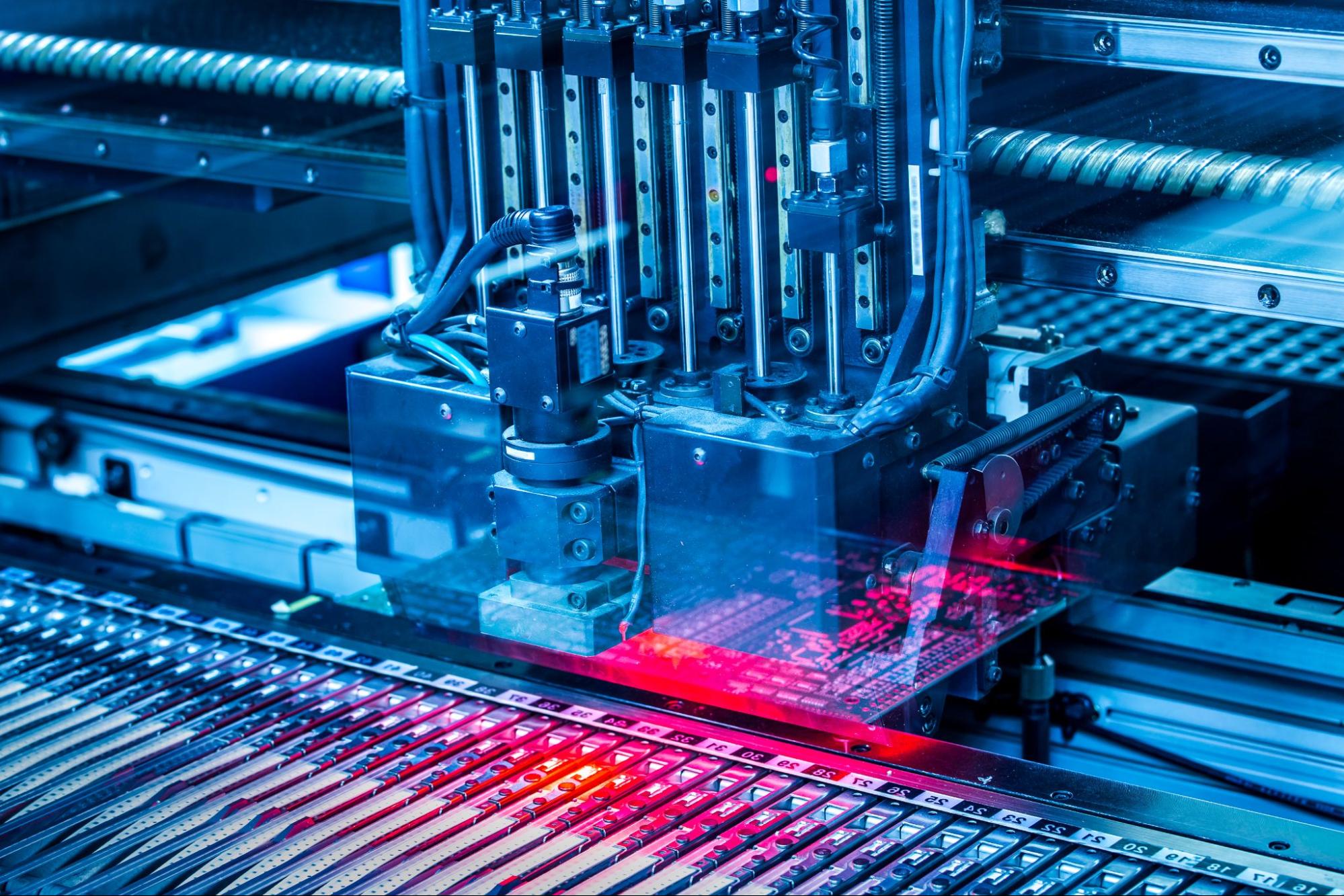
VII. Quality Control and Testing
Now fully assembled, the PCB must be closely inspected for quality. Ideally, problems will be discovered and eliminated before this process stage. However, a final quality check ensures that only the highest-quality products are shipped to the customer.
- PCBs will undergo careful visual inspections for defects, misalignments, and other imperfections.
- Visual inspections are also done with automated optical inspection (AOI) systems that can compare real PCBs to the expected result of the manufacturing process.
- PCBs are also tested for electrical continuity and functionality. This step will identify any final electrical issues with the finished board, such as faulty components or incorrect values.
Imagineering: Superior Production Backed by Competitive Pricing and On-Time Deliver
Take advantage of what our customers already know. Imagineering has the experience and capability to fabricate the highest-quality printed circuit boards. Plus, each project is backed by the service and confidentiality you demand.
Our global buying power provides you with the opportunity to save money. At the same time, our local PCB production allows us to fulfill your more complex and larger PCB orders quicker and more efficiently.
We have taken one-stop PCB manufacturing to the next level. Ready to see the difference with Imagineering? Get a free quote today.
We Have Taken One-Stop PCB Manufacturing to the Next Level
Get your Instant Quote Today