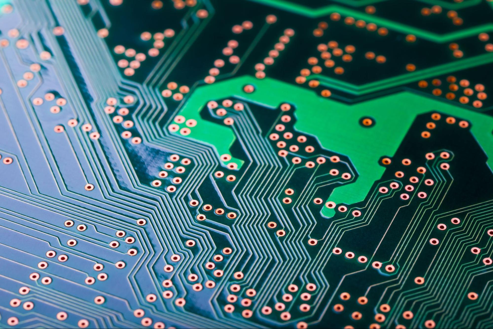
A printed circuit board (PCB) is a medium that connects electronic components in a controlled manner. It has a laminated sandwich structure such that each layer contains circuit traces and other features etched onto sheets of copper. These sheets are electrically isolated from each other with a layer of non-conductive substrate. PCBs are faster and easier to fabricate than earlier mass-producing circuits since fabricators can mount and wire components in a single operation. Furthermore, fabricators only need to create one layout, allowing them to make many PCBs simultaneously.
Fabrication is creating the bare circuit board to serve as the foundation for the PCB during assembly. Choosing your fabricator carefully is essential since even minor errors can render a PCB useless. Communication between the designer and manufacturer is particularly critical in this industry because PCB manufacturers are typically located outside the U.S.
This post provides an overview of the PCB fabrication process, including pre-processing steps. It also covers key considerations for selecting a PCB fabrication company.
PCB Design Process
Understanding the electrical parameters is the first step in designing a PCB. Next, you need to create a schematic that specifies the PCB’s purpose and function at the electrical level. The schematic shows the location of components, so a mechanical engineer can understand how they’ll fit on the intended devices.
PCB design requires using software tools such as OrCAD, Altium Designer, and EAGLE. The best choice depends on your company and design and requires extensive research. For example, OrCAD is a large toolkit with many features and capabilities, making it most suitable for complex designs. Altium Designer performs less than other tools, so you should perform real-world testing to ensure it can handle your design. EAGLE requires users to have an Autodesk Fusion 360 subscription.
Rules ensure a PCB will be easy to fabricate, so they govern every aspect of PCB design. They include electrical, physical, and spacing design rules. Electrical design rules deal with electrical properties such as impedance and voltage. Physical design rules relating to trace width, differential pairings, pads, and vias. Spacing design rules address the clearance and spacing between components.
Generating Manufacturing Data
Computer Aided Manufacturing (CAM) is the use of software to control and automate a manufacturing process. In the case of PCBs, CAM software converts the design into a format that manufacturing equipment can understand. CAM is essential for ensuring that the final product accurately reflects the design.
CAM consists of several distinct steps, beginning with data preparation. This step checks the design for errors and inconsistencies, such as clearance violations, overlapping pads, and trace width violations. Panelization is arranging multiple boards on a panel to increase production efficiency. The next step is to generate tool paths for drilling, routing, and milling by optimizing these tasks for the specific equipment.
CAM software then generates Gerber files from the schematic, the standard format used to manufacture PCBs. The next step is performing a Design for Manufacturability (DFM) check to ensure the design is optimized by checking for problems like undercuts and overhangs. The final step in PCB design is to generate the output files that the fabricator will use to make the PCBs.
PCB Substrate Material
Selecting the best material for the substrate is critical to achieving the best performance from a PCB, including function, longevity, and cost efficiency. This choice also affects your fabricator’s ability to make it, so you must ensure it’s a material they can handle. The materials most commonly used in PCB substrates include the following:
- FR-4
- CEM-1
- CEM-2
- CEM-3
- RF-35
- PETE
- Polyimide
Temperature of Glass-Transition
A substrate’s response to temperature is one of the most important factors to consider when selecting a substrate since overheating is a common cause of PCB failure. This industry uses the glass transition (Tg) temperature for this purpose, essentially the temperature at which the material loses its rigidity. Standard PCBs have a Tg of 130˚C, while high-performance boards have a Tg above 170˚C.
PCB Material Choices
FR-4 is a common choice for PCB substrates since the standard version has a Tg 135˚C. However, other versions of this substrate have Tg values ranging from 150˚C to 210˚C, making them applicable for high-density PCBs. CEM-1, CEM-2, and CEM-3 are also suitable for high-density applications, with Tg values of 122˚C, 125˚C, and 125˚C, respectively. RF-35 has a Tg of 130˚C, so it’s also a candidate for high-density applications.
PFTE, commonly known as Teflon, has Tg values of 160 to 280˚C, making it suitable for high-frequency, high-power PCBs. Polyimide is also a good choice for these applications, with a Tg of 250˚C or higher. These substrates are also preferred for flexible PCBs, as FR4 substrates are pretty rigid.
PCB Manufacturing
The primary parts of a PCB include the substrate, copper layer, solder mask, and silkscreen. The substrate is the primary component and serves as the PCB’s skeleton, providing its core strength. The copper layer is a copper foil or coating that conducts electrical signals throughout the PCB. The solder mask is a layer of polymer that electrically insulates the copper layer, preventing it from short-circuiting. The silkscreen, or the legend or nomenclature, shows information about the PCB.
Once the manufacturer prints the design onto a piece of laminate material, it applies a layer of copper foil or coating. This process bonds the copper to the laminate, creating the PCB’s structure. The manufacturer then etches the copper to reveal the design, leaving only the copper needed to provide the PCB’s required functionality. The inner layers of the PCB will require the additional removal of copper.
The manufacturer then cleans each PCB’s layers before aligning the inner and outer layers using the holes previously punched into each layer. A technician does this by placing the layers onto an optical punch machine, which drives a pin down through the holes to align the PCB layers.
PCB manufacture includes inspections at various points to check for defects. This process is especially important before the layers are laminated because the manufacturer can’t correct existing errors once the layers are bound together. A specialized machine performs an automated optical inspection (AOI) at this point, which compares the PCB with its extended Gerber design. A technician also visually inspects the PCB before passing it for lamination.
Surface Finishing
The surface-finishing stage involves plating the PCB with a conductive material so the manufacturer can mount electronic components during assembly. This plating also covers the copper layer, protecting it from oxidation. Many finishing materials currently exist, each with its own set of trade-offs. The best choice primarily depends on the customer’s budget and the PCB’s specifications.
In addition to their physical properties, designers must consider the legal regulation of materials when selecting a surface finish for PCBs. For example, the European Union (EU) adopted the Restriction of Hazardous Substances Directive 2002/95/EC (RoHS) in 2003. This directive regulates some hazardous substances used in electrical and electronic equipment.
For example, electroless nickel immersion gold (ENIG) is a common surface finish due to its long shelf life and RoHS compliance. However, it’s more expensive than other options. Electroless nickel electroless palladium immersion gold (ENEPIG) has a high solder strength and reduces corrosion, but it requires greater care in processing to achieve the best performance. Using gold and palladium also makes ENEPIG an expensive option for a finish.
Standard hot air solder leveling (HASL) is cost-effective, long-lasting, and reworkable. However, it contains lead, which isn’t RoHS compliant. A lead-free version of HASL is available, which is also cost-effective and reworkable.
Immersion tin (ISn) is a popular option for press-fit applications since it produces tight tolerances for holes and is RoHS-compliant. However, handling the PCB can cause tin whiskers and soldering problems. Due to silver’s high electrical conductivity, immersion silver (IAg) has a low signal loss. It’s also RoHS-compliant, but this finish can oxidize and tarnish.
Hard gold is durable and RoHS compliant but also expensive. Organic solderability preservative (OSP) is RoHS-compliant and cost-effective but has a short shelf life.
Solder Mask and Silk Screen
A solder mask provides the PCB’s copper layer with extra protection from corrosion and oxidation and also gives the PCB a more consistent appearance. This phase begins with a thorough cleaning of the PCB, after which fabricators apply ink epoxy and solder mask film over the entire surface. After that, the PCB is exposed to ultraviolet light, showing technicians where to remove the solder mask. The PCB then goes into an oven to cure the mask.
Fabricators must print vital information directly onto the PCB’s surface in a stage known as the silk screen application or legend printing. This information includes the following:
- Company ID numbers
- Component references
- Manufacturer marks or logos
- Part Numbers
- Pin locators
- Switch settings
- Test points
- Warning labels
Electrical Testing
A technician conducts many electrical tests on the PCB after it has been coated and possibly cured. These tests ensure the PCB’s functionality and test the initial design’s ability to withstand the manufacturing process. Electrical testing of PCBs must comply with IPC-9252, entitled Guidelines and Requirements for Electrical Testing of Unpopulated Printed Boards.
These tests generally consist of circuit continuity and isolation tests. Circuit continuity tests check for PCB circuitry disconnections, commonly known as open circuits or just “opens.” Circuit isolation tests measure the isolation values of the PCB’s components to locate any short circuits or “shorts.”
Technicians also conduct other tests to ensure a PCB’s functionality and basic reliability tests. For example, a “bed of nails” test involves attaching several spring fixtures to the PCB’s test points. These fixtures then apply up to 200 grams (g) of pressure to those points to see if it damages the PCB. The manufacturer may also choose to implement other electrical tests at this point. Boards that fail electrical reliability testing must undergo repair and retesting until they pass these tests.
Final Inspection and Delivery
Technicians score the PCB boards and break them apart to ready them for a final inspection. This check examines several aspects of the boards, such as ensuring the hole sizes match all layers and meets the designer’s specifications. The board dimensions must also match these specifications. Additional inspection items include checking for burrs or sharp edges on the finished board. Fabricators also ensure the boards are free of any dust.
Packaging and delivery is the last stage of PCB manufacturing. These steps include placing packing material around the PCBs to keep dust and other foreign matter away, similar to vacuum packing. After sealing the PCBs, technicians place them into containers to protect them from damage during shipping. The fabricator then delivers the PCBs to the customer.
Partnering with a PCB Manufacturer
PCB fabrication is an exacting process that requires many steps to create a successful end product. It begins with the design phase, which examines the PCB’s electrical parameters to create a schematic. CAM software generates the data manufacturers need to make the PCB, including tool paths. The next step is selecting the best substrate material, which requires the fabricator to balance factors like performance, cost, and longevity.
The fabricator can print the design and apply copper to serve as the PCB’s circuitry. Unneeded copper is then etched away before inspecting the layers with machines and human technicians. Once they pass inspection, the various layers are bound to create the PCB. The fabricator finishes the surface and mounts the components before applying a solder mask and silk screen. After a final round of electrical testing and inspection, the fabricator delivers the PCB to the client.
At Imagineering, we’re committed to providing our clients with the best possible service and support from design to production. Our team of experts is well-versed in the latest PCB trends and can help you find an innovative solution to any problems you have.If you are ready to start, contact us today for a custom quote tailored to your specific needs.


