
Advancements in printed circuit board (PCB) design and the automation of PCB assembly have played a pivotal role in the quality and mass production of a wide range of electronic devices, equipment, and systems. Printed circuit boards have changed how we live and interact within our environment – at home, work, and everything in between. Without the first PCB prototype created in the 1920s, our multilayered boards would not exist.
“The Fourth Industrial Revolution or 4IR…is driven by disruptive trends including the rise of data and connectivity, analytics, human-machine interaction, and improvements in robotics.”
The access to data and the connectivity between devices made possible by the miniaturization and advancement of PCBs drive the Internet of Things, often referred to as IoT.
What is PCB in IoT? The printed circuit is the foundation of every IoT-enabled product worldwide.
In domestic products, printed circuit boards dictate the functions of smart refrigerators and dishwashers, smartwatches and smart TVs, and home systems like HVAC, water, and lights. In modern commercial construction, IoT comprises sensors and controllers that automatically optimize energy usage, monitor security and surveillance, and keep track of scheduled facility maintenance.
Modern manufacturing uses unseen printed circuit boards that enable smart robotics and factory automation located deep within machines performing extremely fast-paced or dangerous tasks.
Continue reading to discover the crucial role printed circuit boards play in IoT devices, making modern life easier to manage, factories safer, and businesses more energy efficient.
What is PCB in IoT?
The IoT consists mainly of PCs that enable internet connection via wireless technologies and incorporate electronics such as processors, sensors, and low-power wireless connectivity components. It’s easy to separate IoT devices into three usage categories:
- Consumer Connected Devices – home appliances and consumer products like wearables
- Enterprise Devices – used in the business sector to automate business processes or monitor facilities
- Industrial IoT – performs complicated or repetitive tasks related to industrial processes or assembly
The world is still on the brink of discovering how advancements in PCB technology will continue to make IoT devices even more versatile. PCB size is still a constraint since PCBs require room for additional features, but PCB designers have developed multiple techniques to help make this possible.
First, consider how this simplified view of IoT technology, which depends on a host of printed circuit boards, could be useful for IoT applications.
- Ability to sense: An IoT device must first recognize its physical surroundings and be able to retrieve data from within the environment.
- Transform data: The data IoT devices receive may be physical and must get transformed into information that computer algorithms understand.
- Communicate: All IoT devices must have a communication channel between devices and controllers.
- Analysis: For true IoT functionality, the collected data must get analyzed, compared, tracked, logged, and much more.
- Control: Finally, there must be a mechanism to output some control over another device to benefit the end user.
From sensing and transforming data to communication, analysis, and control, the role of PCBs remains crucial in enabling the functionality and effectiveness of IoT devices. Let’s dig into how the integration of these components works.
Integration of Components
During the PCB prototype process, stakeholders capitalize on the early design phase to identify and rectify flaws that could prolong the project’s timeline or escalate production costs. All electronic components must integrate into a single board function harmoniously. PCB designers must navigate the rapid evolution of IoT devices, which often feature compartmentalized designs with sub-circuits.
Ensuring the seamless integration of PCBs with other systems becomes a critical consideration in the overall architecture of the device. To achieve best practices and meet industry standards for PCB design and manufacture, adhering to various guidelines, including IEEE, ANSI, NEC, and IPC (formerly the Institute for Printed Circuits), is the most effective approach.
The IPC, an internationally recognized electronics-industry standard, offers comprehensive best practices for every PCB design and production stage.
Effective connectivity is vital for IoT devices to exchange data with other devices. To select the most suitable option, PCB designers must carefully evaluate the advantages and disadvantages of protocols such as Bluetooth, Zigbee, and WiFi. Often, compromises arise due to conflicting technology parameters, including range, latency, and transfer rates.
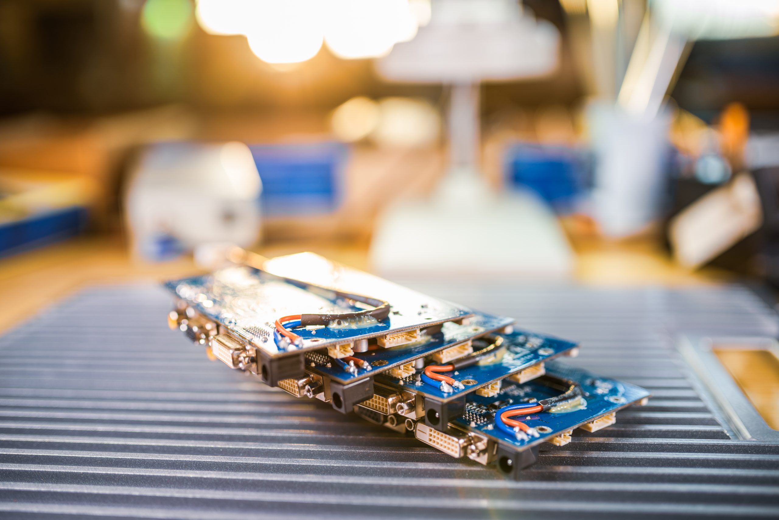
Miniaturization and Space Optimization
As mentioned above, physical space quickly becomes a confining restraint for PCB designers, making PCB miniaturization and space optimization a critical part of the PCB prototype process in IoT devices. Techniques like surface mount technology (SMT) enable component placement in close proximity, allowing IoT devices to be small yet functional.
Wearables, in particular, require tiny PCBs, imposing constraints on layout, space, and weight. Wearables must have very small PCBs due to their size and unconventional shapes. Maintaining the required functionality imposes major restrictions on a PCB’s layout, space, and weight, so the design has to be minimalist.
Power Management and Energy Efficiency
When designing a PCB prototype for IoT devices, consideration must be made for effective power management and energy conservation to reduce the negative effects of electricity-induced heat. Power regulation, energy consumption management, and even power distribution within the device are crucial in extending the battery life of IoT devices – a major concern for both consumers and commercial end-users.
Turning off portions of a device when they aren’t in use is one of the best ways of conserving battery power. This capability requires designers to divide the PCB into functional blocks and allocate a power-consumption budget for each block. Power-regulating ICs that meet space requirements help ensure each block remains within its budget.
Quality Control and Reliability
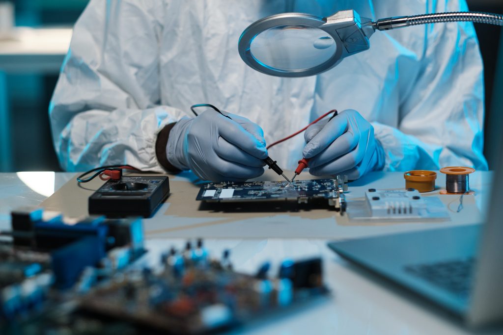
PCB assembly routinely includes quality control (QC) measures to improve the device’s reliability and durability. Manufacturing processes like soldering are essential for IoT devices, where robust quality control is needed to ensure consistent performance. PCBs’ QC procedures get classified into visual inspection and electrical methods.
PCB Inspection and Testing Methods
Today, multiple technologies to inspect printed circuit boards have replaced visual inspection and delivered higher quality assurance. These include Automated Optical Inspection (AOI) and X-Ray Inspection, which can detect solder defects, missing components, incorrectly oriented features, and stains.
PCB prototype providers may also conduct various tests to verify the quality and functioning of a PCB design and assembly. These include in-circuit testing, flying probe tests, and burn-in testing. PCB Functional Testing (FCT Testing) is widely used to ensure the PCB functions as expected. An experienced technician will check for correct voltage and current levels, the temperature of the board under power, and operating frequencies.
Scalability and Mass Production
A robust process for PCB assembly is essential for scaling up the production of IoT devices to meet consumer demand. The mass production of PCBs for IoT applications requires fast output and consistent quality to combat product failure during end-use. Taking a PCB prototype to mass production depends heavily on the products that get mass-produced, printed circuit boards.
Today’s PCB manufacturing can meet consumer demand only because of the fast turnaround of automated machinery and robotics, which include soldering robots, PCB assembly robots, and PCB inspection and testing robots.
“The global consumer IoT market size was evaluated at USD 221.74 billion in 2022 and it is expanding around USD 616.75 billion by 2032, growing at a CAGR of 10.77% from 2023 to 2032.”
An economic market of this proportion is staggering, especially when you consider that at the heart of every IoT device are integrated printed circuit boards, so small, yet holding so much low-voltage electrical power, electronic control algorithms, proprietary data, along with all the communication and connectivity protocols to talk with each other and relay that information to the device owner.
Experience Top-Quality PCB Assembly with Imagineering – Your IoT Solution Partner!
Imagineering is a leading PCB manufacturer specializing in IoT applications, offering flexible and rigid PCBs that meet aerospace quality standards. Our quick-turnaround PCB prototype services ensure reliable performance in critical applications across various sectors. Whether you need prototyping, verification, or total production, Imagineering can help you create the PCB you need for your next project.

Read up on our latest blogs: