
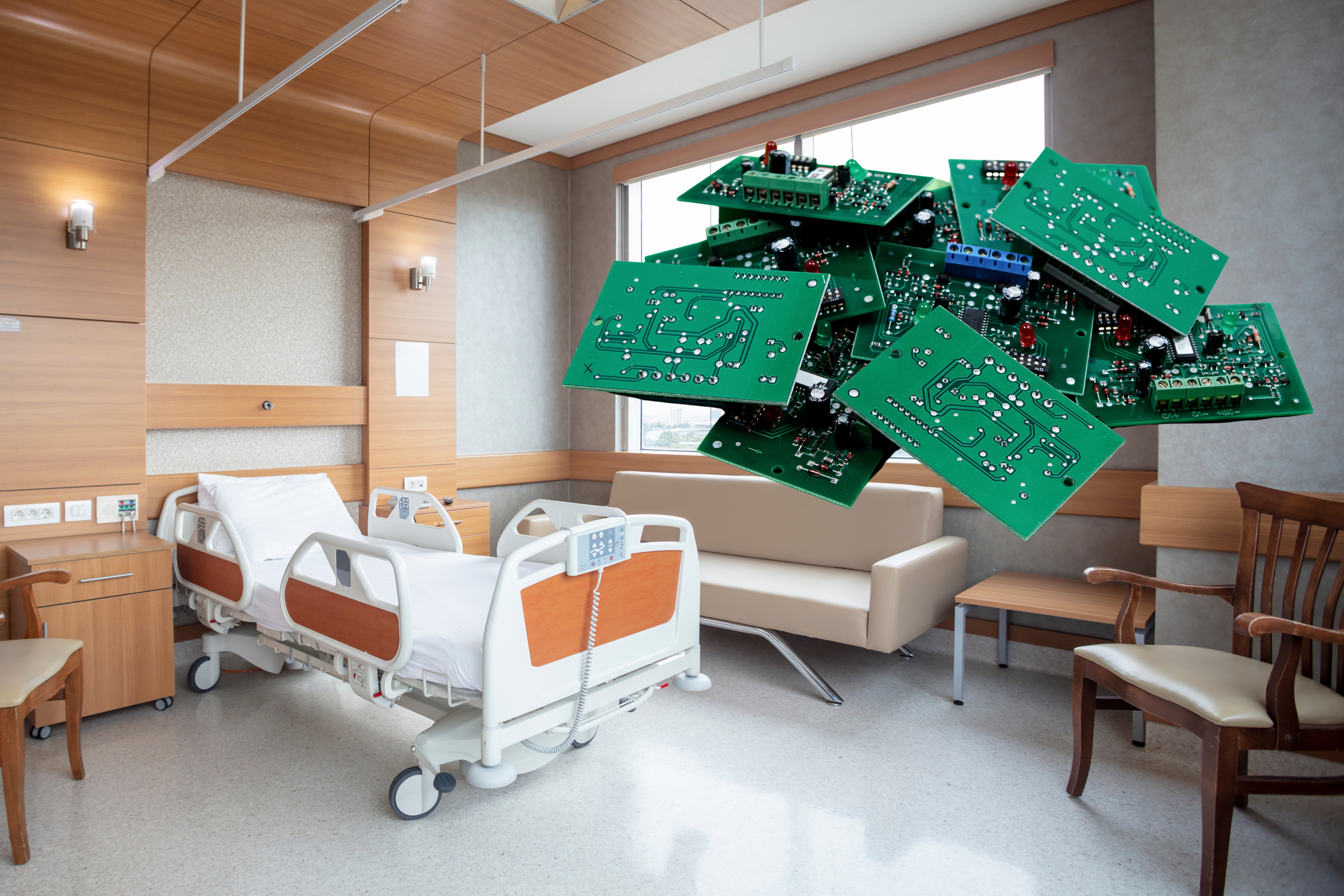
Inside every hospital room, there are devices outfitted with the latest technologies in modern medicine, including printed circuit boards (PCBs), that must be reliable, precise, and versatile to treat patients and get them back to their lives.
Whether you need an x-ray for a broken arm, an infusion for chemotherapy, or a new blood glucose monitor, you and your doctors rely on a well-designed PCB to carry out your treatment effectively and safely.
Where else do PCBs show up in the medical world? How are the latest developments in PCB manufacturing affecting the drive towards miniaturization, new regulations, and emerging technologies?
We’ve put together this guide to help you understand PCBs’ vital role in modern medicine and the medical device industry.
Overview of PCBs in Modern Medicine
Modern medical devices are complex technologies that require a lot of components and specific materials to serve many functions. Like most modern devices, they rely on PCBs to keep their diverse components connected, powered, and reliable for use in hospitals and clinics worldwide.
Examples of medical devices that utilize PCBs are:
- Diagnostic Equipment: X-ray machines, MRI machines, and CT scanners.
- Patient Monitoring Systems: Electrocardiogram (ECG) machines, Electroencephalogram (EEG) machines, and pulse oximeters.
- Implantable Devices: Pacemakers, defibrillators, and neurostimulators.
- Infusion Pumps: Devices that control patient administration of fluids, medication, or nutrients.
- Respiratory Equipment: Ventilators, Continuous Positive Airway Pressure (CPAP) machines, and nebulizers.
- Blood Glucose Monitors: These small devices are critical for managing diabetes.
Each device relies heavily on PCBs for accuracy, data processing, portability, and customizability. PCBs also aid in connectivity features that allow remote monitoring of patients and even facilitate telemedicine.
How PCBs Are Made Precise and Reliable for Medical Settings
Precision and reliability are priorities for any electronic device, but what may be an important aspect of a PCB used in consumer electronics becomes a critical, life-and-death proposition in medical devices.
Here are a few challenges engineers must overcome when designing PCBs for use in medical settings.
Electromagnetic and Radio Interference (EMI & RFI)
Problem: Many electronic devices can generate EMI and RFI in a medical setting. Imaging tools and wireless communication systems can corrupt the accuracy of sensitive medical equipment.
Solution: PCBs can be designed with shielding and filtering techniques, such as ground planes, enclosures, and precise signal routing, to minimize EFI and RFI.
Stringent Temperature Requirements
Problem: Certain medical devices, like surgical lasers, autoclaves, cryogenic freezers, or incubators, must operate in specific temperature ranges for optimal function.
Solution: PCBs are engineered using specialized materials, heat sinks, and thermal vias, enabling efficient heat dissipation. Components can also be efficiently packed to ensure maximum airflow and temperature control.
Strict Regulatory and Compliance Standards
Problem: In critical medical applications, malfunctioning devices can have life-threatening consequences. Strict regulations exist to ensure that medical devices are reliable and can operate continuously for long periods.
Solution: PCBs are designed from the outset with industry-specific standards in mind. These include standards like ISO and FDA regulations. These regulations require PCB manufacturers to engage in risk management and quality procedures designed to identify and mitigate the risks of device failures.
The Miniaturization of Medical PCBs
As with the general technology trend, medical devices are shifting towards miniaturization. Smaller devices are more portable and patient-friendly than the clunky, heavy solutions of the past. However, this miniaturization shift is only possible with the advancements made in PCB technology.

4 Reasons Why Medical Devices Are Getting Smaller
Here are four key advantages to smaller, more portable medical devices:
- Patient Comfort: Less obtrusive devices are more comfortable for patients to wear or use. This leads to improved patient compliance and health outcomes.
- Less Invasiveness: Miniaturized devices are far less invasive. This can improve recovery times and reduce the risk of complications.
- Real-Time Monitoring: Wearable and implantable devices offer continuous real-time monitoring, enabling more accurate and timely data for accurate diagnoses and treatments.
- Accessibility: Miniaturization can make medical technology more accessible to a broader population, including those patients in resource-limited areas.
How PCBs Enable Miniaturization
Modern PCB assembly manufacturers are enabling this shift towards miniaturization with manufacturing techniques like:
- Surface Mount Technology (SMT): SMT allows for smaller, lighter, and more densely packed PCBs when compared to through-hole technology, which contributes to overall device miniaturization.
- Flexible PCBs: Flexible and rigid-flex PCBs offer versatile design options, allowing devices to conform to unique shapes and fit into smaller spaces.
- Multi-Layer PCBs: Multi-Layer PCBs provide more routing options in a smaller space, condensing complex circuits into a more compact form.
- Advanced Materials and Manufacturing Processes: High-performance materials with specific dielectric properties allow for thinner and more compact PCBs, while techniques such as laser drilling enable the creation of intricate PCB designs with smaller traces and components.
With modern PCB technology enabling the trend towards miniaturization, healthcare companies can provide patients with better outcomes using smaller, more portable, patient-friendly devices.
How Medical Devices Integrate into the IoT with PCBs
Medical devices are rapidly evolving to leverage the benefits of wireless communication and integration into the Internet of Things (IoT). This integration is propelled by the latest developments in PCB manufacturing.
Here’s how it’s happening:
Wireless Communications Made Easy
Advanced PCB manufacturing techniques mean wireless communication modules can be integrated directly onto boards.
Technologies like Bluetooth, Wi-Fi, and cellular connectivity are all enabled through these developments.
Sensors Gathering More Accurate Data
Miniaturized sensors can be integrated into PCBs and capture a wide range of patient data, including vital signs, activity, and environmental conditions.
Wirelessly transmitting this data to a centralized system means healthcare providers can better monitor patient conditions and offer better insights.
IoT Connectivity and Cloud Integration
PCBs are now able to incorporate IoT protocols and interfaces. This enables seamless connectivity with cloud-based platforms, centralized data storage, and analytics software and improves accessibility from multiple devices.
Modern PCB Prototyping Means Devices are More Customizable
Prototyping is physically developing a board after it’s been designed. Since no design is perfect the first time, producing a few prototype boards before beginning mass production is important.
Modern PCB prototyping techniques, including quick-turn PCB prototyping, enable better customization and more reliable boards.

Quick-Turn Prototyping Enables Faster PCB and Device Production
Quick-turn PCB prototyping allows medical device engineers to rapidly create and test prototypes of their designs, which accelerates development and enables faster iterations to refine the product.
Through this prototyping process, engineers can quickly tailor customized PCBs to the needs of a medical device. This includes integrating specialized sensors, communication modules, and other components critical for medical applications.
Finally, designers can make incremental improvements to the PCB layout and functionality based on testing results.
Better prototyping means better testing, better iterations, and more effective devices.
How Customized PCBs are Used in Medical Devices
Here are just a few examples of how customized PCBs can be used to improve medical devices:
- Better Sensor Integrations
- Accurate Signal Processing/Amplification
- Wireless Communication and IoT integration
- Efficient Power Management
- Smarter User Interface Control
- Better Data Storage and Data Processing
- More Safety Features and Redundancy
- Customized Form Factors
Through practical applications like these, customized PCBs have become integral to the functionality and performance of medical devices.
3 Predictions for The Future of Medical PCBs
What happens from here on out is far from certain. Technologies develop in ways that we cannot always predict. However, certain avenues of PCB development are currently being explored that may have massive impacts in the next decade.
Here are a few possibilities:
1. AI and Machine Learning Will Become more Prevalent
PCBs will increasingly incorporate specialized chips and processors capable of handling AI and machine learning algorithms. This will enable devices to process complex medical data in real-time, leading to better diagnostics and patient outcomes.
2. Flexible and Stretchable PCBs
We will see PCB technology advance to accommodate flexible and stretchable substrate materials. This will revolutionize the design of wearable medical devices, allowing them to conform to the body’s contours for improved comfort easily.
3. Energy Harvesting Techniques
PCBs will integrate energy-harvesting components like piezoelectric materials and solar cells to capture ambient energy and power low-energy medical devices. This will reduce the reliance on traditional batteries and contribute to more reliable devices.
Prototyping with Imagineering
PCB technology is developing rapidly, and the medical industry will benefit from these advancements. Everything from efficient use of energy to better data collection and analysis and better patient compliance through more comfortable devices hinges upon the progress of PCB technology.
To learn more about how Imagineering is helping to push the PCB industry into this exciting era and to stay on top of the latest developments, check out our blog frequently.
Looking for a PCB manufacturer to prototype your latest design? Talk to us. Let Imagineering guide you through the process of a quick-turn prototype and get your device ready for production within the week.