
Few pieces of technology are as versatile and common as the printed circuit board (PCB).
These wafer-thin electronic boards serve as the foundation for nearly every piece of modern technology we use every day.
Given the massive number of applications that PCBs must be able to accommodate, there are also a massive number of production methods and forms that PCBs can take.
Today, we’ll discuss one such method and form: the double-sided PCB.
We’ll explain everything, from what a double-sided PCB does to what it looks like to produce a double-sided PCB and the benefits of using one on your electronic devices.
What is a Double-Sided PCB?
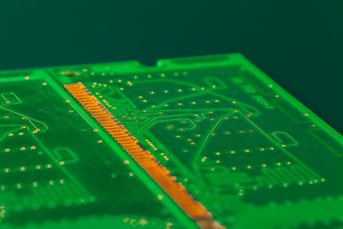
Double-sided PCBs are printed circuit boards that have conductive copper layers on both surfaces. These surfaces are separated by a dielectric material, but manufacturers make use of vias (tiny holes) to connect circuits between the two sides.
Thanks to the vias, double-sided PCBs enable more complex circuits than single-sided PCBs without greatly adding to the size of the board.
Double-sided PCBs are useful anywhere that densely packed circuitry and efficient use of space is valued. Examples include:
- LED lighting
- Power supplies
- Hard drives
- Automotive dashboards
- Consumer electronics
- & more
Double-sided PCBs are a versatile option for any electronics manufacturer looking for a space-efficient design that still facilitates complex circuits without resorting to multi-layer PCBs.
How Double-Sided PCBs are Manufactured
Manufacturing double-sided PCBs is a complex process that shares many similarities with the manufacturing of traditional PCBs but with some key differences.
Here’s an overview of the process where we’ve highlighted the parts of the process distinct to double-sided PCBs:
Design & Materials
Like traditional single-sided PCBs, the process starts with a design and DFM check that finds and rectifies any flaws in traces, holes, or component placements.
A substrate material is then selected from a variety of options. FR4 is a common choice due to its flame-retardant properties and availability.
It’s important that the final substrate material has copper on both sides to make it suitable for a double-sided design.
Drilling
Since a double-sided PCB will have components on both sides, there needs to be a way to connect circuits on one side of the board to the other side. This is done by drilling tiny holes, or vias, through the board.
There are multiple techniques for drilling holes through PCBs, but the one used for double-sided PCBs is known as a plated through hole (PTH).
A PTH is a via that is plated with copper on the inner side of the hole. After drilling, the hole is simply exposed to epoxy, which is unsuitable for circuits. Copper plating is necessary to allow electrical currents to flow from one surface to the other, hence the “plated” through the hole.
To achieve this, manufacturers use a process known as electroplating.
Imaging, Printing, and Etching
Next, a photo resistive film is printed which contains the design of the circuits. After applying the film, the board is exposed to UV light, which hardens the parts of the board that will eventually contain the circuits. This is done for both sides of the board at the same time.
At this point, the entire board is covered in copper, which means the entire surface is conductive instead of just the desired pathways.
To achieve the desired circuit pathways and eliminate the excess copper, the board is passed through what is known as an etching solution. This solution removes the excess copper from the board, except for the copper which was hardened by the UV light from the previous step. This remaining is what forms the electrical pathways along both surfaces of the PCB.
At this point, the pathways are ready for automated optical inspections (AOI).
Assembly
Once the pathways have been verified as correct, the board is ready for assembly. From this point, each side of the double-sided PCB will be loaded with the appropriate components according to the design and are connected to one another with the copper pathways formed in the previous steps.
The Pros and Cons of Double-Sided PCBs
Double-sided PCBs are a significant evolution from their single-sided counterparts. They manage to expand the surface area for components without resorting to multiple layers, which can be a more expensive and complex production process.
Benefits of Double-Sided PCBs
There are 3 main benefits of double-sided PCBs:
- Enhanced Circuit Density
The double-sided nature of these boards doubles the surface area available for components. This feature is particularly beneficial for devices that require more circuitry without a proportional increase in size.
- Improved Versatility
This increased space for components allows designers more flexibility and freedom to create complex circuit pathways, enabling the integration of more features into the device without enlarging its footprint.
- Long-Term Cost-Effectiveness
Although they initially may cost more, double-sided boards are more cost-effective in the long run, especially for devices that require complex pathways that might otherwise have to use multi-layer PCBs.
Potential Drawbacks
There are some reasons you may want to consider other options than a double-sided PCB. Some of the drawbacks of these boards are:
- Manufacturing Complexity
Double-sided PCBs are naturally more complex to produce than their single-sided counterparts. The additional steps, such as through-hole plating, can lead to higher initial production costs and longer lead times.
- Heat Dissipation
High-density components can lead to problems with heat management. Effective thermal regulation is essential but can present serious challenges in the design phase.
- More Complicated Designs
In some ways, allowing for more complexity in the design phase is obviously a good thing. However, increasing the number of options for circuit pathways also demands greater design skills and software. Errors in double-sided designs are more difficult to diagnose and rectify.
Choose an Experienced Double-Sided PCB Manufacturer—Choose Imagineering
Double-sided PCBs are an excellent and cost-effective option for anyone looking to create compact and powerful electronic devices, assuming you have the design skills and manufacturing technology necessary to utilize them.
Regardless of your experience level, if you’re considering using a double-sided PCB in your design, you’ll want to choose a PCB assembler with the expertise needed to make your product idea a reality.
Imagineering is here to help.
We have the technology and expertise to craft PCBs of all shapes, sizes, and layouts, including double-sided PCBs. Contact us today and let us know what you’re thinking of creating.