
In the 1960s, a swift increase in the complexity of electronic devices necessitated the development of printed circuit boards that allowed more wiring and electrical circuits in a small area. Hence, the multilayer PCB was born.
Though multilayer PCBs are not new, the technology underlying them has continued to progress over the last several decades. Today, the multilayer PCB stands as a perfect option for designers of complex electronic products across a wide range of industries.
In this post, we’ll discuss:
- How multilayer PCBs are manufactured.
- The design considerations that engineers have to make.
- A general cost comparison between multilayer PCBs and their single and double-layered counterparts.
Before we get into those topics, let’s talk about the defining characteristics of multilayer PCBs.
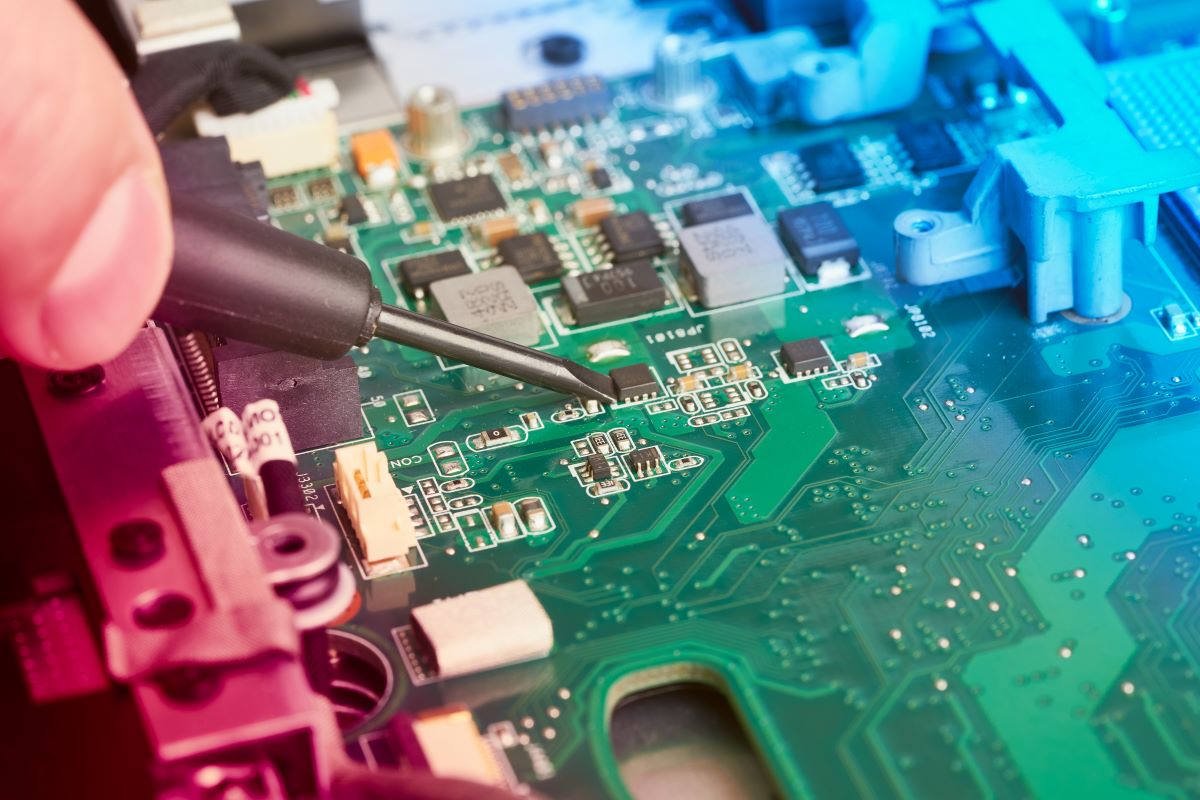
Understanding Multilayer PCBs
Layers are the primary defining feature of multilayer PCBs. Compared to single—or double-layer PCBs, they allow the boards to accommodate more circuits in a smaller footprint.
Multilayer PCBs are characterized by their:
- Layer Composition: Multilayer PCBs typically consist of a series of interconnected layers, including signal, power, and ground planes. The layers are sandwiched between sheets of insulating material to prevent electrical interference and physical damage.
- Applications: When space and weight are at a premium, multilayer PCBs shine. They are common in high-speed circuits like those in computers, smartphones, and GPS technology.
- Construction: Each layer of a multilayer PCB can act independently, carrying distinct circuits with interconnections made possible through drilled holes.
This is what helps multilayer PCBs serve as the foundation for a wide range of complex electronic functionalities.
The Multilayer PCB Manufacturing Process
Like all PCB manufacturing, multilayer PCB manufacturing is a complicated process. It’s rife with potential pitfalls and opportunities to get things wrong or damage the board.
Modern PCB manufacturers have developed intricate techniques that help them design and produce these boards quickly and to a high standard. It looks something like this:
1. Inner Layer Processing
In the first phase, copper-coated substrates are covered with a photosensitive film that, when exposed to light, hardens where the circuit layout dictates.
The substrate is then ready for a process known as etching. Here, the unexposed film is chemically removed. Next, the exposed copper is etched away. This leaves behind only the circuit pattern.
2. Lay-up and Lamination
Construction of the inner layers involves stacking alternating layers of pre-etched circuit boards and insulating materials on top of one another. Alignment is secured by pins that ensure each layer is precisely positioned.
The stack is then subjected to heat and pressure, causing the insulating layers to melt slightly and fuse the stack into a single entity.
3. Drilling Vias and Through-Hole Plating
The stacked boards are then ready to be drilled. The holes created in this step are known as vias. They will electrically connect the various layers of the board.
After drilling, the walls of the holes are non-conductive exposed substrate. To make them conductive, they undergo a process known as through-hole plating. This makes them conductive, linking the layers together with an electrical pathway.
4. Outer Layer Processing
Finally, the outer layers can be processed, and the entire board is finished.
Similar to the inner layers, the outermost layers are coated, exposed, developed, and etched to form the outer circuit patterns.
Additional finishes, such as gold plating or solder mask application, are added to protect the copper from corrosion and to insulate the surface.
Each phase demands meticulous attention to detail to avoid errors that could affect the performance of the final product. To ensure a reliable and repeatable process, every decision made during assembly is ultimately decided in the design process.
Design Considerations for Multilayer PCBs
The design phase is where engineers ensure a board is as efficient as possible while also aiming to optimize the manufacturability.
Here are a few key considerations designers make for multilayer PCBs:
- Layer Configuration: Deciding the number and order of layers based on the circuit complexity and the electrical requirements of the application.
- Material Selection: High-frequency applications may need advanced materials like Rogers or polyimide to ensure signal integrity and thermal stability.
- Trace and Space: Managing trace width and spacing is critical in preventing crosstalk and ensuring signal integrity, particularly in high-speed circuits.
- Via Types: The use of through-hole, blind, or buried vias affects both the performance and cost. Designers must balance the need for compact designs with manufacturing capabilities and costs.
Each of these factors will make a strong impact on the final performance of the PCB. With careful and deliberate planning, designers can maximize functionality and minimize costs.
The Cost of Multilayer PCBs
If there is a downside to multilayer PCBs, it’s that they can be more expensive overall than their single—and double-layered counterparts. However, manufacturers who choose multilayer PCBs do so for their increased versatility and performance, which compensates for the increased cost.
Key factors influencing the cost of multilayer PCBs include:
- Layer Count and Complexity: More layers increase costs due to more materials and longer production times.
- Materials Used: Specialty materials like high Tg FR-4 and polyimide are more expensive but necessary for high-performance boards.
- Production Volume: Higher volumes can reduce the cost per unit, offering economies of scale.
- Technological Requirements: Advanced techniques like HDI or the use of microvias add to the cost.
Imagineering Specializes in Complex, Multilayer PCB Assembly
For electronics manufacturers striving to compete in a constantly developing marketplace, multilayer PCBs represent a useful piece in their arsenal of design tools.
Their increased functionality makes them more difficult to produce, which can increase costs. But their performance and versatility more than makeup for this initial investment.
Electronics manufacturers looking for a PCB assembler who can produce multilayer PCBs according to a wide range of specifications and materials can rely on Imagineering for their next product cycle.
For decades, Imagineering has helped our customers design, build, and mass-produce multilayer PCBs for electronics products in industries ranging from medical to aerospace.If you want to learn more about how our assembly process can improve your multilayer PCBs, contact us today.