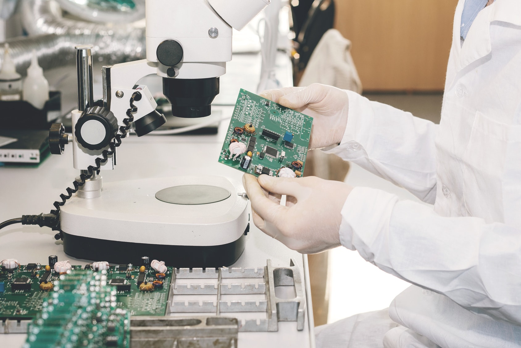
Since the late 80’s video cameras have been reducing in size along with the cartridges they contain in order to fit in the palm of your hand. Technology has continued to move forward to the point where computers are lighter and faster than ever. This has been possible with the advancements of printed circuit boards (PCBs).
PCBs have been shrinking in size which puts PCB fabrication houses under pressure to continue this trend of smaller and denser chips and make sure all the circuitry is running off these smaller chips.
PCBs and HDI
When it comes to PCBs, one of the technologies that has really changed the game for the amazing downsizing transformation is High Density Interconnect (HDI). HDI increases the functionality of PCBs while using the same or less amount of board’s real estate. It makes it possible for these devices to be smaller in both weight and size while being able to do more than their predecessors. Specialty mini-components, thinner materials and equipment have allowed for electronics to shrink while improving speed and quality.
HDI technology offers designers the opportunity to use both sides of a PCB rather than just one. Components that are made smaller in size are able to take up less real estate on the PCB and be closer together. Decreased component size and pitch allow for more I/O in smaller geometries. In turn, this setup increases the speed of signal transmission while greatly reducing the potential for crossing delays and loss of signal.
VIPPO Structure
The increasing usage of HDI printed circuit boards makes the plugging of micro-vias an important aspect of PCB manufacturing. As HDI design is becoming predominant and component pitch is becoming finer, PCB designers are opting for via-in-pad plated over, also known as VIPPO or POFV, structure.
The benefit of moving to VIPPO is that it helps the PCB assembly perform optimally while saving room, especially when blind vias are used. To make via-in-pad possible, the PCB fabrication process includes a step to plate the via holes and fill the plated vias with epoxy before the via is then covered up with a plated copper. However, these steps take extra time and require additional materials.
The Future of PCBs Fabrication
PCBs are expected to shrink by half every year for the next 10 years. As a result, the pressure is on PCB manufacturers to keep up with consumer demand by finding other ways to reduce the size of PCBs through either their manufacturing processes or the materials. It’s not unexpected to see this pressure when it comes to increasing the amount of processing power possible. Therefore, more and more logic will need to be added on a particular size board while still being able to perform at higher clock rates.