
Behind the technological marvels of the 21st century, the HDI PCB is certainly one of the greatest contributing factors to our increasingly digitized world. A byproduct of the drive towards miniaturization, the HDI PCB is used in everything from smart devices to rocket ships. It has also made these much cheaper to manufacture and assemble.
What is a HDI PCB, and what differentiates it from standard printed circuit boards? In this blog, we cover the basics and benefits of HDI printed circuit boards, and the manufacturing capabilities to create HDI PCBs in short order.
What is a HDI PCB?
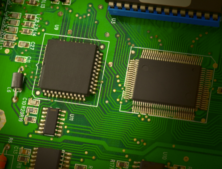
A high-density interconnector (HDI) PCB is a circuit board with a higher wiring density per unit area compared to more conventional boards. They are constructed out of a number of layers of conducting materials that are separated by a dielectric material, which are glued together by adhesives and linked by microvias. By definition, these constitute any printed circuit board with an average of 120-160 pins per square inch.
HDI PCBs have finer spaces between lines, higher connection pad density, and more parts assembled onto a smaller surface. They rely on microvias in order to function. With many layers that must communicate with each other in order to properly function, the condensation of parts relies on extremely small parts delivering electrical signals from one layer to another. Microvias are a specialized type of via with a hole diameter of 150 microns or less that allow this kind of printed circuit board to function.
What are the Benefits of a HDI Printed Circuit Board?
The primary benefit to using an HDI PCB comes from the push towards miniaturization. Prior to their invention and popularization, electronic devices were limited by the size of the printed circuit boards directing them. This is most clearly seen in early mobile phones, devices about the size of a brick with substantially diminished functionality compared to the smartphones of today.
With the demand for more real estate on the surface of a circuit board, HDI PCBs were able to make much greater use out of limited surface area. An HDI PCB offers benefits such as:
Size – Portable devices as we know them today would not be possible without printed circuit boards. Packing a big punch for its small size, HDI PCBs lower the number of layers required to manufacture a PCB, leading to technology we can wear and put in our pockets.
Lower Cost of Materials – Thanks to the significantly diminished scale of a HDI PCB, they use far fewer materials with better performance power than other types of printed circuit boards. From a production standpoint, this equates to larger amounts of revenue.
Faster Prototyping – The lead times to creating a HDI PCB are shorter, leading to less time spent designing and testing prototypes.
Faster Signal Transmission – As HDI PCBs take up less space than their counterparts, electrical signals have less distance to travel. These boards have less signal loss and crossing delays.
Higher Heat Resistance – HDI PCBs are sometimes used in high-temperature applications that require them to function in extreme conditions. By design, they have a higher comparable heat resistance.
Requirements for HDI PCB Manufacturing
Special manufacturing techniques are required to fabricate and manufacture HDI PCBs. Finding a manufacturer that meets these standards, as well as the ability to do so on a quick-turn basis, are crucial for implementation. This includes:
- Laser Direct Imaging
- Laser Drilling for Microvias
- Blind & Buried Vias
- Stacked & Staggered Vias
- Sequential Lamination
At Imagineering, Inc., we have the tools and capabilities to quickly produce and deliver HDI printed circuit boards for a variety of applications. Our specialization in rigid and flex double-sided and multilayered PCBs makes us suitable for any number of PCB fabrication and assembly needs. Trust your fabrication and assembly needs with state-of-the-art production capabilities that offer aerospace quality and standard prices. Our capabilities include:
- Turnaround in as little as 24 hours
- High mix low-to-mid volume
- Class II and Class III inspection
- AS9100D certified and ITAR compliant
- Leaded and lead-free RoHS assembly
- 100% on-time guarantee
Do you have a HDI PCB project you need completed now? Contact us today for more information about our services.