
The downside with a schematic is that they don’t prove wether or not a design works. With a printed circuit board you can put your design to the test.
The worldwide market for printed circuit boards is growing at a rapid rate of 11% per year. It’s expected to be worth $72.6 billion by 2022.
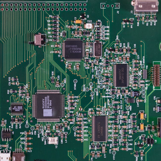
These products make up the core of almost all our favorite electronics. If they’re not designed properly, the function of our phones, cars, and more can suffer.
A circuit board schematic is like the blueprint of a house, letting the designer know how many of each component to use, where they go, and what they do. They’re a critical component of the PCB design process and an important part of the testing phase as well.
Read our guide to find out how to design a printed circuit board and how a schematic can help you test your layout.
PCB Schematic Symbols
There are several symbols you’ll need to know if you want to read and design a circuit board schematic.
Resistors are represented on a schematic by zig-zag lines or a plain rectangle. If the design requires a potentiometer or variable resistor, the symbol will also have an arrow in the middle.
Most resistors only need two terminals, but a potentiometer needs three.
Polarized capacitors get a curved plate to represent the cathode and a plus sign to represent the positive pin.
Inductors show up on a circuit board schematic as curved bumps, looped coils, and/or filled rectangles.
Switches come in various types with different symbols to represent them.
An SPST or single-pole/single-throw switch is the simplest option. It’s represented with two terminals and a half-connected line for the actuator.
More complex switches have more lines representing more connections to the actuator. There may even be more than one actuator in complex switch setups.
Remember to include a symbol to indicate the power source of your printed circuit board design. You can choose direct current or alternating current sources, batteries, or voltage nodes.
Diodes show up as a triangle against a straight line. They have a positive anode terminal and a negative cathode terminal distinguished with a plus and minus sign.
Light-emitting diodes add a few lines pointing in the opposite direction. Photodiodes put arrows pointing towards the diode.
Integrated circuits show up as rectangles with pins sticking out of them. Each pin needs a number and a function.
Each component of your printed circuit board’s design should have a value and a name. The value tells an important characteristic like how much power a component uses. Names are a combination of letters and numbers, such as R1 for the first resistor and C1 for the first capacitor.
Reading and Designing a Circuit Board Schematic
There are also other ways to make reading a circuit board schematic easier in addition to knowing and including all the necessary symbols.
Nets show which components are wired together. It’s best to color-coded them and give them a name that indicates their purpose.
Junctions show where wires split in two different directions. They’re represented by nodes, shown with dots placed at the wire intersections. If there’s no node, the wires are just passing each other, but if there is, they’re connected.
The best printed circuit board designs will also have blocks of similar components placed together. All the power sources might be in the same place, for example.
A voltage node helps you name components that share the same voltage and lets you know that they’re all connected. The ground voltage is one of the most important because several printed circuit board components need a grounded connection.
How to Design a PCB
It’s possible to design your own PCB with enough knowledge and practice. Start by finding the best CAD design software for your needs. Then, create an effective schematic and use it to put the components together.
Make sure to consider every element of the final product in your printed circuit board schematic. Think of how far apart components need to be, how you’ll distribute power, etc.
Remember that your work isn’t over once you’ve got a working printed circuit board schematic. You still have to consider several important factors as you place each part.
Poor heat dissipation causes about 50% of PCBs to fail. Power generators, cars, and lights have high thermal loads. Use metal cores to keep components cool.
Be careful that your printed circuit board designs meet their intended purpose. Prototypes and final products require vastly different designs.
Consider cost as you design your PCB. Reducing the number of components or replacing them with cheaper options can save you time and money in the long run.
While you can design your own PCB, hiring someone else is sometimes best. They’re experts with the experience to make sure nothing goes wrong.
Learn more about different printed circuit board design processes, including DFM or design for manufacturability and full turnkey and consignment assembly.
Testing a PCB
No matter how you design your printed circuit board, it’s critical to test it to make sure all the components work the way you want them to.
You can test a PCB in a variety of ways. These include visual inspections, performance tests in extreme conditions, in-circuit tests, and a manufacturing defect analysis or MDA.
You can also use the circuit board schematic itself. Use it to make prototypes and check that every component is exactly where it needs to be.
You can even reverse-engineer circuit board schematics if you have the finished product in front of you. Draw the components on a piece of paper or create a design in a photo editing program using the proper symbols. This can help you find out how a printed circuit board was designed and where problems may be coming from.
If you don’t test your design before sending it off to the public, it could arrive with a range of defects. There are several methods, including using your circuit board schematic to help you. Learn more about the importance of PCB testing here.
Where to Get a Well-Designed PCB
A printed circuit board schematic is the heart and soul of the design process. Using symbols and images, it lets engineers know exactly where each component needs to go and what it should do.
It’s easy to design your own PCB and test it as long as you have a carefully drawn circuit board schematic. You can also test it using the schematic as a guide.
Hiring an expert makes the process easier, and we have a variety of printed circuit board products for you to check out. Check out our current specials and get a quote today.