PCB warping is a problem that can have expensive consequences if not addressed early on. Unfortunately, it is all too common, and one of the biggest headaches for PCB designers, fabricators, and manufacturers across the globe.
When a printed circuit board experiences warpage, it no longer retains a flat profile, typically curling at the ends. This can lead to significant problems down the line:
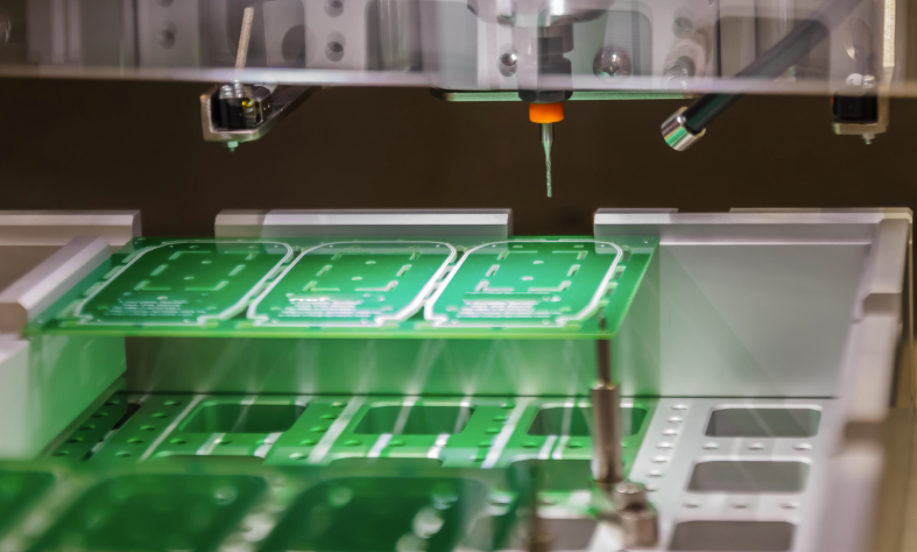
- Pick-and-place machines are designed for flat surfaces. When a board has warped, these machines may inaccurately place components onto the face of a PCB.
- Wave solder machines can flood the board with solder when it curves inward, acting like a basin and pooling the solder.
- Warped PCB boards may not fit inside of the end product. Even if the board is still theoretically functional after warping, it cannot be manufactured at scale in this state.
As these issues illustrate, PCB warping can destroy a batch of manufactured boards, wasting time and money. Thankfully, the reasons for PCB warping are well known, and can be prevented before manufacturing and assembly. In this blog, we analyze what causes PCB warping, as well as steps that can be taken to avoid this costly mistake.
What Causes PCB Warping?
Printed circuit boards can become unusable after warping too much. However, every single PCB will show some degree of warping due to the nature of their manufacturing process. Generally speaking, any warpage under 0.75% is considered in range for industry specifications, although this may differ depending on the end use of a product. This warping is generally invisible to the untrained eye.
PCB warpage occurs due to the presence of imbalanced copper percentages in different layers of the board. Laminate is made out of several different types of materials: resin, glass fibers, and copper. Although these layers are flat, they also have “locked-in” stress – when heated to extremely high temperatures, thermal expansion causes movement in the direction of that stress. PCB board layers thus need to account for this movement in a balancing act.
In multilayer printed circuit boards, it is thus essential that the layers of copper are properly balanced around the central layer, and distributing equal amounts of weight around the center helps minimize the warpage.
The amount of warp and weft associated with different prepregs can be calculated in advance to prevent major warpage. The closer a prepreg’s warp fill is to another, the less chance for warpage, whereas prepregs with significantly different warp fills in the x and y directions create the potential for warpage.
As soon as a board begins warping, it will continue to warp further throughout the soldering process thanks to the introduction of heat activating the locked-in stress of the board.
Other causes of warping include:
Heat Sinks and PCB Warping – Warping primarily occurs during preheating, and can also occur during the soldering process which applies localized heat to specific areas of the board. But warping isn’t only specific to these stages. When a PCB has heavy heat sinks, it can result in localized expansion on the printed circuit board and can sag during the transition phase.
Operating Temperatures – When printed circuit boards are fabricated, they will undergo several periods of intense heating and cooling. Fabricators must be careful to minimize this processing time as much as possible, while evenly heating both sides of a board. A good fabricator will communicate with the manufacturer to ensure they understand warp and weft directions before lamination.
Fixing PCB Warpage
Once a printed circuit board has become warped, it is nearly impossible to fix. Thus, the best method for fixing PCB warping is by mitigating risks that cause it from the start through smart board design, as well as an understanding of the importance of thermal management in PCB manufacturing.
In this section, we address several of the methods printed circuit board fabricators and manufacturers employ to avoid or fix PCB warpage.
Designing Around Warpage
The best way to avoid warpage is to design printed circuit boards with the potential for warpage in mind. As stated previously, all printed circuit boards will warp to some degree, but the amount to which they do is dependent on created balanced designs. A couple of ways to do this include:
- Balancing layers of a multilayer printed circuit board so that layer thicknesses are symmetrical along the center of the printed circuit board.
- Using the same supplier for prepregs and core sheets to ensure the coefficient of expansion is similar.
- Matching the outermost layers on both sides of a printed circuit board to match each other. If they copper areas on both sides differ significantly, their thickness will be uneven, causing warp.
Pallets and Fixtures
One method PCB manufacturers have historically used is a pallet that clamps down the board during the manufacturing process. For those who have used watercolors, this method may be familiar. After applying watercolor paints to paper, the sides will generally curl up on themselves unless they are taped down. This logic applies to printed circuit boards in a superheated environment by pinning the corners down and preventing warpage from occurring through side clamping the vertical and horizontal planes.
Unfortunately, this method has limitations. This type of fixture slows down the PCB manufacturing process, adds additional costs, and reduces flexibility in a high mix environment.
Plate Flattening
Some manufacturers have specialized machines for flattening out boards that deviate too far from the norm. These machines, however, can only be used at certain points during the manufacturing process – once a PCB has been completed, the warpage is permanent. While methods for flattening boards are used by some manufacturers, the effect is often not great, and it can rebound after it has been flattened.
While tools for plate flattening exist and are used, their effectiveness is limited. Thus, the role that proper PCB design takes is critical for ensuring the best yield.
Addressing Environmental Factors
Improper storage of substrates can lead to increased risk of warpage. Particularly in environments with high humidity, copper clad laminates can absorb moisture. Moisture-proof packaging can help reduce this risk, but if this is unavailable, minimizing humidity in warehouses can help prevent this from occurring.
Additionally, when plating is pressed by heavy objects, it can increase warpage overall. For these reasons, it is essential that storage conditions are monitored in advance.
Work with Imagineering
PCB warping is one of the biggest causes of delays and lower yields of printed circuit boards. It is a major problem for manufacturers, and while design is one of the primary reasons for warped printed circuit boards, it can be attributed to a multitude of factors. Thus, finding a printed circuit board expert that you can trust is the only way to ensure the best results.
At Imagineering, we pride ourselves on our 100% guaranteed rapid turnaround times. We provide aerospace quality manufacturing at standard prices, as well as offering same-day turnaround for prototyping and production in as few as seven days. We are AS9100D certified and ITAR compliant, and offer multilayer, rigid, and flex PCBs.
PCB warping is a problem across the industry, but with our expertise and turnaround times, we can ensure you get the most value for your yield. Contact us today for more information about our services.