
Printed circuit boards are expected to be both functional and reliable throughout their lifespan – PCB inspection is essential for ensuring that the finished result is working at optimal capacity with no room for failure. Medical, aerospace, and military applications require an exacting degree of precision from printed circuited boards, with many lives depending on their functionality. Yet even simpler printed circuit boards have undergone more extensive inspection methods over the years to ensure the best quality results.
Today, a variety of PCB inspection methods are employed to ensure the best printed circuit board quality is available, although the kinds of testing used vary depending on the cost and complexity of the project.
In this blog, we examine common PCB defects, and outline several of the most commonly used testing methods available on the market.
What is PCB Inspection?
In short, PCB inspection is the act of mitigating errors or mistakes that may have emerged during the fabrication and assembly processes. This is done through a series of procedures that have largely become automated.
PCB inspection is required throughout multiple stages of the assembly process. After a printed circuit board has been fabricated, an inspection is done to seek out any shorts or defects that might be present before shipping. A second inspection occurs after PCB assembly components have been attached to the board.
The IPC has set guidelines for what constitutes an acceptable board. The IPC-A-610 inspection standard is used for assembly inspection, while the IPC-A-600 is used for bare board inspection.
Depending on the class of circuit board being produced, more stringent rules around testing must be followed. Class 3 printed circuit boards, the same used in commercial jets, space shuttles, and high temperature PCB environments, have no margin for error, and thus have the highest inspection frequency.
The Evolution of PCB Inspection Methods
The first printed circuit boards were much simpler than the designs we see today. Containing far fewer solder connections and components, the primary form of inspection was called MVI, or manual visual inspection. This process was as simple as looking over a board and ensuring all of the components were connected in the right place.
As the complexity of printed circuit boards has grown exponentially over the years, manual visual inspection has grown out of practice. This method was seen as easily prone to failure thanks to human error, and produced substandard board quality as the complexity of printed circuit boards spiked. When not caught early, defects lead to faulty boards that become increasingly more difficult to fix as the board proceeds down the assembly line, leading to higher costs and greater amounts of waste from faulty boards.
To reduce human error, the visual inspection process has become largely automated. Paired with surface mount technology, inspections can proceed at a much higher rate with greater degrees of accuracy. As surface mount technology has led to smaller PCBs and multilayered design, other tools like X-rays are required to find early detection of faults.
What are some of the most common types of PCB inspection available today? We investigate the topic in depth below.
Types of PCB Inspection
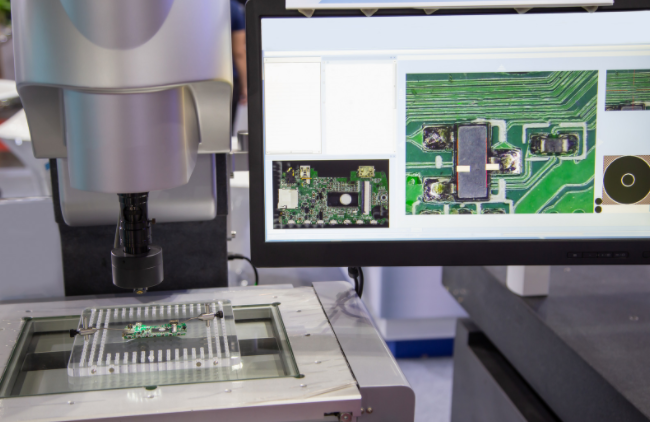
Automated Optical Inspection (AOI)
Automated optical inspection uses cameras to take photos of a printed circuit board and compares them against detailed schematics to ensure that there are no mistakes on the board. The board is lit from various angles and several pictures are taken and assembled together to build a complete profile of the board.
It is particularly useful for detecting issues early in printed circuit board manufacturing, such as scratches, nodules, stains, thinning solder, open circuits, and short circuits. AOI systems can also detect incorrect or missing components.
3D cameras have recently found use in AOI systems to provide even more reliable results. This is of the utmost importance to height-sensitive devices, as 2D camera systems rely on colored lighting and side-angle cameras to achieve these results.
AOI is able to detect the most common PCB faults, and is a ubiquitous system in PCB manufacturing. Often, AOI systems are deployed at several points throughout a facility to detect errors early. However, as these systems are designed around cameras, they are limited by what they can visually detect. 3D cameras have an advantage in that they can detect height differences, but they are unable to inspect hidden connections that are found in multilayered boards. For boards that are densely loaded, they may be unable to inspect components that are hidden or shadowed.
As a result of these drawbacks, AOI is not the only inspection method employed by most printed circuit board manufacturers. Especially in Class 3 PCB manufacturing, inspection must be flawless, leading to the development of additional inspection technology.
X-Ray Inspection (AXI)
With the advent of surface mount technology, or SMT, smaller components have led to more densely populated boards with over 20,000 solder connections. Solder connections on these boards are small enough that they can’t be inspected by AOI equipment. Further, multilayered boards contain components that cannot be visually detected from the surface. X-ray inspection is able to provide a far more detailed picture of a printed circuit board than what can be done by simply examining its surface.
Printed circuit boards have the advantage of being made from much lighter elements than the solder connecting them. This allows for these details to appear with a high degree of clarity on X-ray inspections. X-rays pass directly through objects rather than relying on visible light – eliminating errors that might emerge from shadows or hidden components.
Why aren’t X-ray inspections used for all PCB inspection purposes? As it is a newer technology in the world of PCB manufacturing, it is expensive to purchase and use, making it unnecessary for lower class printed circuit boards that lack the complexity found in new chip packages. It requires experienced operators to use these machines, and the process can be extremely time consuming, leading to added expenses for customers.
PCB Defects Found Through Inspection
PCB manufacturing is just as much an art as a science, and while the stakes for PCB manufacturing are higher than ever, plenty of defects and errors can emerge in the process. The most common errors are related to solder paste deposition. An excess of solder causes bridged circuits and shorts, rendering a printed circuit board non-functional.
Catching defects early in the PCB manufacturing process is the soundest way for reducing costs overall. While inspection is an invaluable tool in rectifying errors before they grow disproportionately expensive, they must be used in tandem with PCB testing methods to ensure that the boards are functional. For instance, while AXI systems are able to capture virtually all soldering defects, some component defects can only be found through testing the board directly.
Imagineering Inc Uses Top Tier PCB Inspection to Rout Defects
A printed circuit board is only as good as the components it is built out of. At Imagineering, we understand that failing to use proper PCB inspection methods not only yields ineffective products, but for highly sensitive applications, puts lives in danger.
We follow the practices of our AS9100D certification, ensuring that following exacting guidelines is the only way to ensure success. This means utilizing advanced inspection and testing techniques to ensure only the best results.
Imagineering gets the job done on time, every time, providing best-in-class boards at affordable pricing. Contact us today to learn more about our services.