
When you’re designing a modern circuit board, space is tight, expectations are high, and failure isn’t an option. That’s where surface mount technology (SMT) comes in.
In this blog, we’ll break down why SMT isn’t just a more efficient way to build a board, but the very technology that makes high-density PCB designs possible in the first place:
- Why SMT is the foundation of modern PCB manufacturing
- The top benefits of SMT for high-density PCB designs
- Real-world examples across industries
- Trends shaping the future of SMT
- How to find the right partner for your next board build
Let’s start by looking at why SMT became the industry default.
Why SMT Is Essential for Today’s PCB Designs
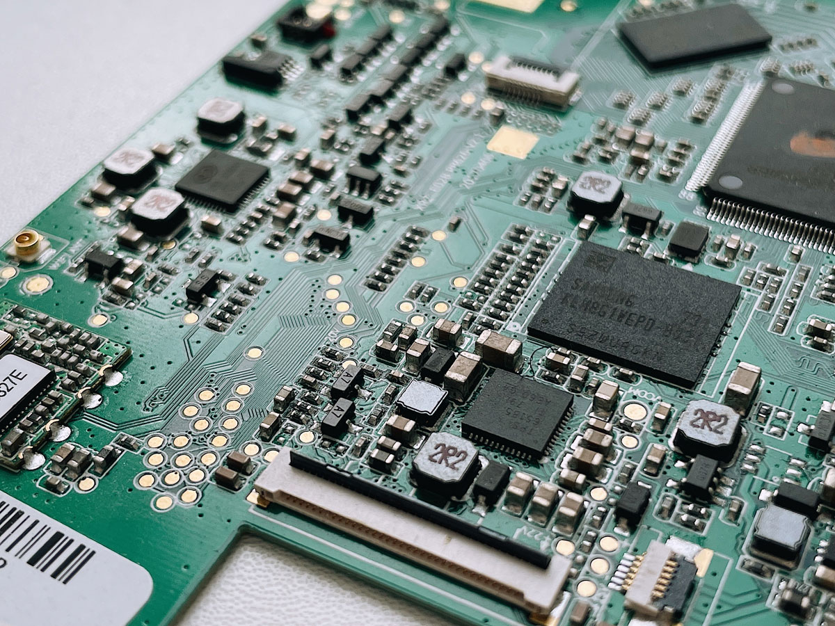
There’s a reason surface mount technology (SMT) is the industry default. When you’re working with high-density PCB designs, the old-school through-hole method just doesn’t cut it. SMT skips the drilling, skips the bulky leads, and gets straight to the business of placing components directly on the board’s surface. That means smaller parts, tighter layouts, and more circuitry per square inch.
In fact, over 90% of all PCB designs today use SMT. The end result is not just saving space but actually making complex electronics manufacturable.
What Makes SMT So Effective for High-Density Layouts?
It’s a combination of precision, speed, and sheer volume. Here’s why SMT wins:
- Tiny components: You can fit dozens, sometimes hundreds, of micro-sized parts into a compact footprint.
- Double-sided population: SMT lets you mount components on both sides of the board, doubling usable space.
- Automated assembly: High-speed pick-and-place machines install thousands of parts per hour, all with micron-level accuracy.
- Better signal performance: Shorter leads and lower parasitics keep high-frequency signals clean and efficient.
SMT makes smaller designs practical, which means it’s invaluable in a world where electronics are only becoming more complex.
The 5 Core Benefits of SMT in High-Density PCB Designs
Surface mount technology is convenient, but beyond that, it solves real problems that engineers face when space is limited and performance can’t be compromised. Below are five major reasons SMT is the gold standard for high-density PCB designs.
1. Miniaturization and Maximum Component Density
This is SMT’s superpower. The components are tiny–think 01005 packages (that’s 0.4 x 0.2 mm)–and they don’t need leads punched through the board. That frees up serious real estate.
Even better, you can mount components on both sides of the board. Double the surface area, without making the board any larger. This is how today’s devices cram in sensors, ICs, passives, and still leave room for thermal management.
2. Faster, More Scalable Production
Speed matters. SMT allows automated pick-and-place machines to run at full tilt, placing tens of thousands of components per hour with micron-level accuracy.
That efficiency pays off whether you’re building 5 prototypes or scaling to 500,000 units. And by ditching the need for drilling holes, you skip a costly, time-consuming step in fabrication.
Here’s what SMT simplifies in the production flow:
- No drilling or lead forming
- No manual component insertion
- Faster soldering via reflow ovens
- Fewer touch points = fewer errors
All of that adds up to lower costs, faster turnaround, and way less human error. That’s a win from both an engineering and business standpoint.
3. Better Electrical Performance, Especially at High Speeds
High-density PCB designs often carry high-speed signals. If your signal integrity is weak, your product fails. SMT helps avoid that.
Shorter lead lengths = lower inductance and capacitance. That translates to cleaner, faster signal transmission, tighter impedance control, and fewer headaches when you’re designing for RF, 5G, or high-speed memory.
It also helps with power distribution. SMT allows you to place decoupling caps practically on top of the ICs they support, minimizing voltage droop and keeping noise under control
4. Stronger Thermal and Mechanical Reliability
In small, dense layouts, heat gets trapped fast. SMT fights back by letting components sit closer to copper pads that wick away heat. The low-profile packages also spread thermal loads more evenly across the board.
And don’t underestimate mechanical resilience. SMT solder joints are solid. They’re better at surviving shock, vibration, and repeated use than you’d expect for such tiny parts.
Some of the physical stress SMT designs can handle include:
- High-frequency vibration (like in vehicles or drones)
- Repetitive mechanical shock
- Thermal cycling from extreme temperature swings
- Long-term exposure to humidity and dust
This reliability is exactly why SMT is used in aerospace and medical gear, where failure isn’t an option.
5. More Design Flexibility and Smarter Layering
SMT makes it easier to implement advanced board technologies like HDI (high-density interconnect). That means microvias, fine-pitch routing, and stacked layers—all tricks for fitting complex logic in a tight footprint.
It also opens up layout options that simply don’t exist with through-hole parts. Want to sneak a ground pour under a BGA? SMT makes it possible. Trying to route 200 nets in four layers? SMT plus HDI gives you a shot.
That kind of flexibility is a game-changer for engineers who need to deliver more functionality in less space.
Where SMT Shines: Real-World PCB Designs in Action
SMT isn’t just a lab darling, but the backbone of real deal, high-performance hardware. If your product needs to be compact, fast, and reliable, SMT is doing the heavy lifting behind the scenes.
Concrete Examples of SMT in Real-World PCB Designs
Take electric vehicles, for example. Their battery monitoring systems rely on SMT boards that pack 100+ components per square inch. That density means more sensors, better control, and smarter power management without adding bulk or weight.
Here are just a few more environments where SMT-based PCB designs dominate:
- Consumer tech: Phones, tablets, wearables
- Automotive systems: Battery control, infotainment, ADAS
- Medical devices: Portable monitors, diagnostic tools
- Aerospace and defense: Navigation modules, avionics
- Industrial automation: PLCs, robotics, vision systems
The reason is simple: SMT lets you pack more function into smaller, more durable hardware. And in a market where space is money and reliability is everything, that’s essential.
What’s Next for SMT and High-Density PCB Designs?
We’re seeing a surge in ultra-fine pitch components, HDI stack-ups, and embedded passives that are all designed to squeeze more capability into tighter spaces. This is especially true in wearables, 5G infrastructure, and IoT devices, where every square millimeter counts. SMT enables these trends by offering the precision and scalability needed to support next-gen complexity without inflating costs or board size.
Even the manufacturing side is evolving. SMT lines are getting smarter with AI-driven inspection, real-time feedback, and better integration with design tools. That means fewer defects, faster iterations, and more room for innovation at the layout level.
The bottom line is that if your future depends on compact, high-performance PCB designs, SMT is the path forward, and it’s accelerating.
To stay competitive now and in the future, you’ll need a PCB manufacturer who knows the tech inside and out.
Why Imagineering Is the Right Partner for Your PCB Designs
As high-density PCB designs continue to evolve, SMT remains the key to unlocking smaller footprints, faster performance, and smarter manufacturing. From component density and thermal control to signal integrity and production scalability, the advantages are too big to ignore.
At Imagineering, we specialize in turning complex design challenges into real-world solutions. Our SMT assembly lines are built for precision, speed, and flexibility–perfect for companies pushing the limits of what modern PCBs can do.
Whether you’re scaling up a commercial product or prototyping a next-gen innovation, we’re the SMT partner that brings engineering insight and manufacturing expertise to every project.