
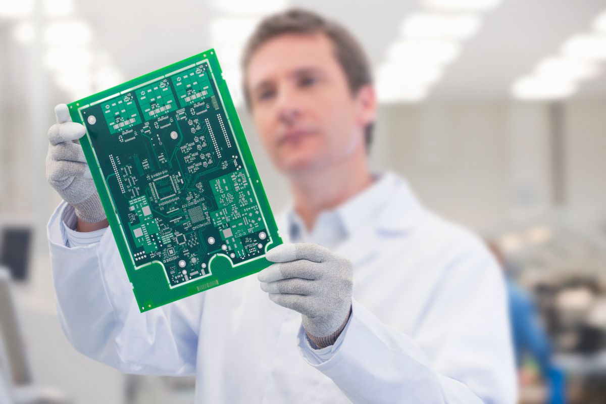
A finished circuit board may look flawless while still hiding a defect that threatens performance, reliability, or long-term durability. That is why PCB inspection is not a single final checkpoint, but a series of targeted evaluations performed throughout fabrication and assembly.
This guide explains:
- The most common defects found in circuit boards
- How manual inspection, SPI, AOI, and X-ray inspection work
- Where electrical and functional testing fit into quality control
- How manufacturers choose the right combination of inspection methods
Understanding these processes can help buyers evaluate manufacturing partners, reduce avoidable failures, and make better decisions about quality requirements. It starts with a clear understanding of what PCB inspection methods are designed to accomplish.
What Are PCB Inspection Methods, and Why Do They Matter?
PCB inspection methods are the visual, imaging, measurement, and electrical processes manufacturers use to identify defects before a board reaches the customer. Checks may occur after fabrication, solder-paste printing, component placement, reflow, or final assembly.
Inspecting at multiple stages matters because early defects are usually easier and less expensive to correct. A misplaced component or poor solder deposit may be reworked immediately, while the same issue discovered after assembly can cause scrap, delays, or field failures.
Inspection and testing serve different purposes. Inspection looks for physical or measurable defects, while electrical and functional testing verifies connectivity and performance. The more complex or safety-critical the application, the more rigorous the inspection plan should be. Aerospace, medical, automotive, and industrial boards often require broader coverage, tighter acceptance criteria, and better traceability than a simple consumer prototype.
What Types of PCB Defects Can Inspection Find?
PCB inspection methods are designed to catch several broad categories of defects:
- Component defects: Missing parts, incorrect values, reversed polarity, misalignment, lifted leads, and tombstoning.
- Solder defects: Bridges, opens, insufficient or excess solder, cold joints, voids, and head-in-pillow connections.
- Board defects: Damaged traces, plating problems, delamination, warping, contamination, and solder-mask irregularities.
Solder defects deserve particular attention because many begin before components are even placed. Peer-reviewed research has estimated that approximately 60% of soldering defect problems in surface-mount assembly can be attributed to the solder-paste stencil-printing process. That does not mean 60% of all PCB defects start there, but it does show why solder-paste inspection is such an important early quality-control step.
Once poor paste deposition passes through reflow, it can produce bridges, opens, tombstones, and weak joints across multiple components. Catching those problems before placement or reflow gives manufacturers a better opportunity to correct the process instead of repairing finished boards.
What Are the Main PCB Inspection Methods?
No single inspection method can reveal every defect. Manufacturers usually combine several techniques based on board design, component density, production volume, and reliability requirements.
Manual Visual Inspection
A trained operator examines the board using magnification, checklists, design files, or a known-good reference board. This method can work well for prototypes, low-volume builds, cosmetic checks, and unusual components.
Its effectiveness declines as components become smaller and assemblies become denser. Human fatigue can also affect consistency, and inspectors cannot see joints hidden beneath packages.
Solder Paste Inspection
Solder paste inspection takes place after stencil printing and before component placement. A 3D SPI system measures the paste’s height, area, volume, and alignment on each pad.
Because printing errors can create downstream solder defects, SPI allows manufacturers to clean the stencil, adjust settings, or repeat a poor print before reflow.
Automated Optical Inspection
AOI uses high-resolution cameras and controlled lighting to compare the board against programmed criteria or design data. It can identify missing or misaligned components, polarity errors, tombstones, solder bridges, and other visible assembly problems.
AOI is fast and repeatable, but it cannot reliably inspect joints hidden beneath BGAs, QFNs, and similar packages.
Automated X-Ray Inspection
AXI uses X-rays to examine internal structures and solder joints that optical systems cannot see. It is especially useful for BGAs, QFNs, dense assemblies, multilayer boards, and high-reliability products.
X-ray inspection can reveal voids, missing solder balls, hidden bridges, opens, and head-in-pillow defects. Because the equipment is expensive and inspection may take longer, manufacturers often apply it selectively to complex or high-risk areas.
How Do Electrical Tests Complement Visual PCB Inspection?
Optical and X-ray inspection can reveal physical defects, but they cannot always confirm that a circuit works correctly. Electrical testing adds another layer of coverage by checking connectivity, component values, and board performance.
- In-circuit testing: A custom fixture contacts test points to detect shorts, opens, missing components, incorrect values, and other electrical faults. It is fast for volume production but requires fixture design.
- Flying-probe testing: Programmable probes move between test points without a dedicated fixture. This suits prototypes and low-volume runs, although each board takes longer to test.
- Functional testing: The board is powered under simulated working conditions to verify inputs, outputs, communications, and other intended functions.
These methods do not replace visual inspection. They complement it by identifying electrical or operational problems that may leave no visible evidence.
How Do You Choose the Right PCB Inspection Methods for Your Board?
The right inspection plan depends on the board’s complexity, production volume, end use, and consequences of failure. Key considerations include component density, hidden joints, required IPC class, cost, schedule, and application risk.
A typical layered process may look like this:
- Inspect solder paste before component placement.
- Use AOI after placement or reflow to find visible defects.
- Apply X-ray inspection to BGAs, QFNs, and other hidden or high-risk joints.
- Perform in-circuit, flying-probe, or functional testing as required.
Simple prototypes may need a lighter combination of manual inspection and flying-probe testing. Dense production assemblies may justify inline SPI, AOI, selective X-ray, and dedicated electrical fixtures.
The strongest quality programs do not expect one system to find everything. They combine complementary methods so physical, hidden, electrical, and functional defects are addressed at the most practical stage.
Choose the Right PCB Inspection Methods With Imagineering
Effective PCB inspection depends on matching the right method to the right stage of production. SPI can identify solder-paste problems early, AOI can catch visible assembly defects, X-ray inspection can reveal hidden joints, and electrical testing can confirm connectivity and performance.
Together, these methods help reduce rework, improve consistency, and prevent defects from reaching finished products. The right inspection plan will depend on your board’s complexity, production volume, application, and reliability requirements.
Imagineering combines advanced inspection and testing capabilities with experienced engineering support. Partner with our team to build an inspection strategy that catches problems early and keeps your PCB project moving forward.
Quick Summary
PCB inspection methods help manufacturers identify visible, hidden, electrical, and functional defects before finished boards reach customers. This guide explains how manual inspection, SPI, AOI, X-ray inspection, and electrical testing work together to improve quality and reliability.
PCB Inspection Method FAQs
Automated optical inspection is one of the most widely used methods because it can quickly identify visible component and solder defects. It is often combined with SPI, X-ray inspection, and electrical testing.
No. AOI relies on cameras and cannot reliably inspect solder joints hidden beneath BGAs, QFNs, and similar packages, so manufacturers typically use X-ray inspection instead.
No. Inspection identifies physical or measurable defects, while testing verifies electrical connectivity and functional performance.