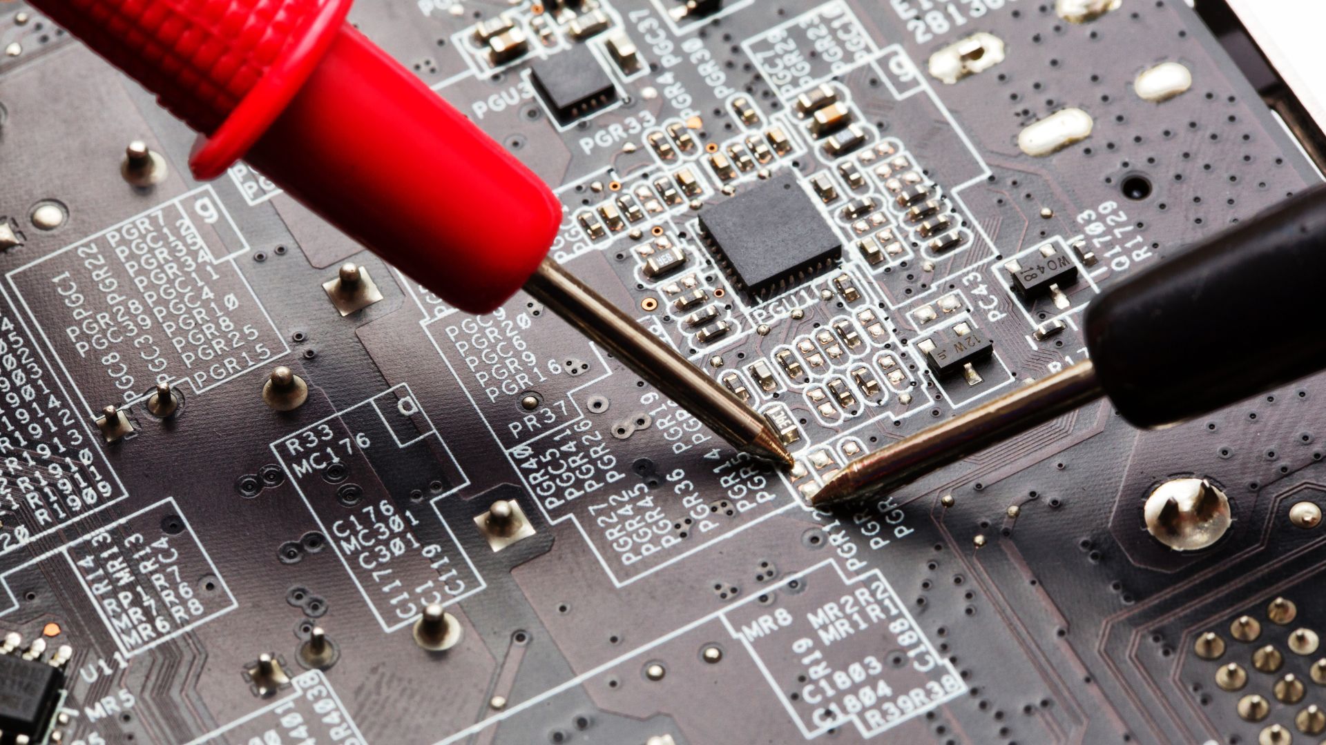
Printed circuit boards are a crucial component for many electronic devices and are favored across manufacturing industries. PCBs are lightweight, heat resistant, and long-lasting, and are used in high-tech equipment like aero-space technology and medical devices. Since PCBs are frequently used in high-stakes situations, their functionality and quality is of the upmost importance.
But how do manufacturers inspect complex and densely designed PCBs? Instead of disassembling the component, X-ray inspection allows manufacturers to monitor PCB quality without damaging or deconstructing the circuit board. Here’s what you need know about the benefits of using x-ray technology in PCB inspection.
How Does X-Ray Technology Work?
If you’ve ever been to the dentist or broken a bone, then you’re probably somewhat familiar with x-ray technology. X-rays penetrate the outer layers of an object, providing a picture of the internal components. X-ray photons pass through materials differently depending on their atomic density, weight, and thickness. Generally, x-rays are absorbed more easily by denser materials, creating a clear image, whereas x-rays aren’t absorbed as well by lighter materials, making them harder to capture.
Since PCBs are primarily made from denser metal components, they are simpler to capture with an x-ray. This allows manufacturers to view the interior structure of a PCB and identify potential issues.
Why is X-Ray Inspection Ideal for PCBs?
As technology has improved, PCB design has grown increasingly complex. PCBs are valued for their compact design and efficient circuitry, but unfortunately, these benefits can make PCBs difficult to inspect without compromising their structural integrity.
Layered PCBs – Adding layers to a circuit board improves efficiency and functionality and is a preferred design for compact boards. But layers by definition obscure interior components, and make manual inspection nearly impossible. X-ray inspection is ideal for layered boards in order to reveal elements like inner solder joints.
Compact PCBs – If a PCB is highly compact, it may be impossible to separate elements without compromising the board. X-ray images provide a clear view of tightly placed components without risking unnecessary damage.
Small PCBs – PCBs are used in devices of all shapes and sizes, and some boards need to be extremely small to fit inside certain appliances. X-ray imaging helps manufacturers zoom in on the interior components of a micro-sized board.
What Common Issues Do X-Rays Reveal?
X-ray tools coupled with image magnification capabilities has transformed the way manufacturers conduct quality control surveys.
Here are some of the most common issues to look for in PCBs using x-ray imaging:
- Solder Voids – In a complex PCB design, individual elements are connected through soldering. Without stable solder connections, circuit boards are liable to malfunction down the line. Solder voids are areas where the connection quality is sub-par due to quality issues with the solder paste. Solder voids may cause boards to malfunction due to poor heat conductivity. X-rays are one of the easiest ways for manufacturers to spot solder voids.
- Solder Bridges – Solder bridges occur when compact soldering elements create an unwanted connection. Since components on small PCBs are often tightly grouped, it can be difficult to see potential issues in soldering without enhanced imaging. X-rays allow manufacturers to view soldering spots that would otherwise be obstructed.
- Pin-Hole Fills – Elements on a layered PCB are often connected by through-holes or pin-hole fills. Pin-hole fill malfunctions are difficult to see, which makes x-ray technology ideal for assessing potential issues.
High Quality Circuitry Built to Get the Job Done
At Imagineering, we specialize in high-quality circuit board manufacturing and design. We offer rigid and flex double-sided and multi-layered PCBs custom designed to meet your requirements. We are proud to offer our clients same-day turnaround for prototyping and production in as few as 7 days, emphasizing our commitment to quality service and quality products.
At Imagineering, we offer aero-space quality circuitry at affordable prices. Whether you need fabrication, prototyping, consignment services, or turn-key assembly, we are here to provide you top-notch results and unbeatable savings. Plus, with our in-house team handling logistics, manufacturing, and delivery, you never have to coordinate production across multiple providers.
With quality you can trust end-to-end service, Imagineering is an industry leader in custom PCB fabrication. Interested in working with us? Contact us today to get started.