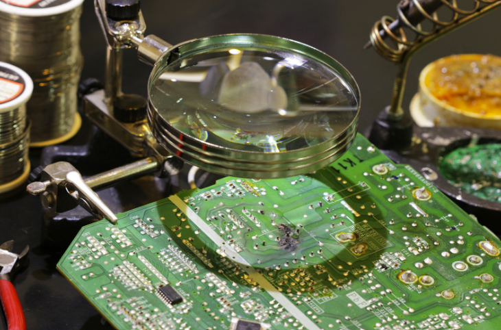
Lamination voids, also known as delamination, are a problem that can occur in the printed circuit board manufacturing process. Errors in printed circuit board manufacturing not only produce malfunctioning boards – they can also cost you valuable time and money.
While these defects can be difficult to diagnose, thankfully there are several solutions that can be used to ensure that you are getting the highest quality of printed circuit board delivered on time.
In this blog, we identify how lamination voids occur, and how high-quality printed circuit board manufacturers avoid this costly error.
What is a PCB Lamination Void?
Producing printed circuit boards requires a high degree of knowledge regarding the interactions between materials, chemicals, and high temperatures. A lamination void is a printed circuit board defect that occurs when the bond between prepreg and the copper foil is weak. Prepreg is the adhesive that bonds the core and layers of a PCB together. When the printed circuit board delaminates, the two separate from each other, forming a pocket.
PCB007 Magazine makes a point to differentiate a PCB lamination void from PCB blistering. Blistering generally occurs on the solder mask layer, which does affect performance but is largely an aesthetic issue. Delamination occurs deeper within a printed circuit board, directly influencing the interlaminar bond strength.
This can have serious consequences for the end user through technical malfunctions, and is further problematized by the fact that it can be difficult to determine why the defect is occurring without examining each layer of the board.
Why Does Delamination Happen?
Delamination has become more prevalent over the years due to the demands being placed on printed circuit board manufacturers as well as the temperatures required to make PCBs today.
Moisture control in printed circuit board manufacturing has increasingly become a problem throughout the industry at large. Miniaturization has caused devices to become significantly smaller, increasing their overall sensitivity. With most global manufacturing outsourced to Southeast Asia, a notoriously humid environment, extra precautions need to be taken to de-humidify the manufacturing space. Compiled with the extra machinery required to remove moisture from devices, delamination is not only a major problem facing manufacturers today, but the problem is only becoming clearer with time.
Although moisture may be the biggest reason why we’re seeing an increase in delamination, it can also be a fault of the design itself. The relationship between each part of a printed circuit board is extremely sensitive to fluctuations. Additional reasons delamination can occur include when:
- The coefficient of thermal expansion between different materials doesn’t match.
- The prepregs and the core’s grain direction are not aligned.
- Lamination parameters are improperly calculated.
- Foil is improperly distributed.
- Drill values are incorrect.
How to Prevent Lamination Voids
The biggest culprit of delamination is when moisture is trapped between layers. It is not an inner layer treatment process issue, but rather is related to the quality of the resin and its potential to absorb moisture. To prevent lamination voids from occurring, inner layer drying is recommended.
Before inner layers are bonded, it is highly recommended that they are oven dried to wick away excess moisture. This helps the prepreg during its curing process.
Lamination voids can also occur when pockets of air get trapped during the lamination process. As the board lamination size increases, the void ratio increases with it. Increasing the resin pressure can help reduce the prevalence of air pockets from forming.
Avoid PCB Defects with a Trusted Manufacturer
Printed circuit board manufacturing is a fickle process. As boards have grown more advanced, they have also become more sensitive to error and environmental factors. That’s why finding a trusted printed circuit board manufacturer has become more important than ever to ensure that you’re getting the best value delivered on time, every time.
To produce boards for aerospace, military, and medical applications, nothing less than perfection is acceptable. Imagineering Inc. specializes in producing the highest quality printed circuit boards. With an AS9100-D certification and meeting IPC Class 3 Standards, every board we make goes through rigorous testing and quality control to ensure optimal results.
Go beyond costly errors and defects in printed circuit boards. Contact us today to get a quote on your next project.