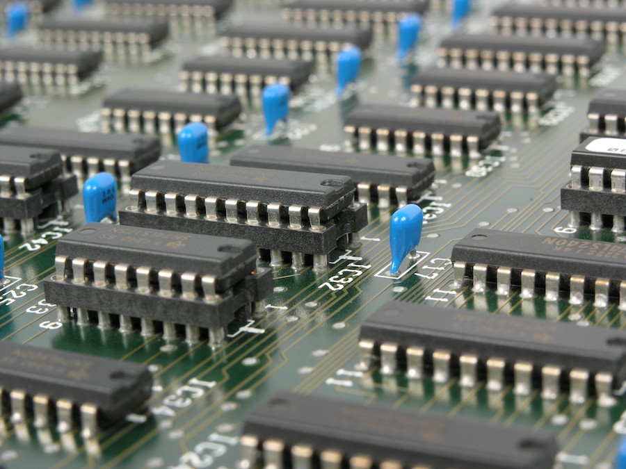
Understanding printed circuit boards (PCB) is a fundamental aspect of computer design. You’ll need to get accustomed to these green sheets and how they work if you ever hope to build a working computer or another electronic device.
But when it comes to creating a PCB, the process isn’t as simple as you might think. There are many intricacies to PCB board design that need to be considered if you’re looking to optimize your board.
Luckily for you, the experts here have outlined some of the most critical parts of printed circuit board layout so that you don’t have to go it alone. This guide will show you some essential tips and tricks to remember when designing a PCB.
PCB Board Layout: It All Starts With a Schematic
When designing a PCB board layout, you need to be as prepared as possible. Firstly, you’ll need to know what it’s used for before going too much further; take a look through our previous blog post if you’re unsure.
Once that’s out the way, you need to get planning. Designing a PCB is not unlike planning the architecture of a house. You need to know which pieces go where and how everything fits together, as well as how many layers your board will be and the materials to use.
Because of that, you shouldn’t immediately start designing the PCB directly. Instead, it would help if you drew up a schematic.
Your schematic should include all the components you know you’ll require. It should also fit the dimensions of the space in which your PCB needs to match; otherwise, you could be building a board that’s simply too big to be used.
Make sure to create a concept that designates which components need to be connected and the rules that must be followed in the overall design. A design flow chart is ideal for this.
Once the schematic and design flow chart have been finalized, you can start thinking about the PCB design itself.
The Right Kind of Component Placement and Routing
It would be best if you had considered the component placement necessary during the design phase. But there are ways of adequately placing components to optimize the overall design of your PCB.
You need to consider components as well as the routing of connections. Make sure never to design a circuit board layout where connections have to cross, as this can cause an overlap in signals that may ruin your design.
A great rule to follow in power outlets is to design with the star-configuration in mind, rather than daisy-chain your connections. If you daisy-chain, that means your connections are running from one component to another.
This means the power has to run through the earliest component first and can result in individual components not getting enough voltage. With a star-configuration, the power will be connected separately to each part of your PCB that requires power.
This then ensures power is distributed equally, and no concerns are surrounding the voltage of the PCB.
If your PCB does have layers, the right way of trace routing is to exchange directions between layers. This can help to prevent any cross-wiring on each separate layer.
Spacing Out Your PCB
When designing a circuit board layout, you also need to consider the space offered to you overall. You should know how much space you have based on the detailed schematics made in the earlier section.
It would be best if you tried to space components out where possible, allowing for direct access to the critical nodes. This is to ensure the copper wiring can reach all parts of the PCB comfortably. It also avoids any chance that your PCB short-circuits due to traces connecting because they were too close to each other.
As a general rule, the more pins a component has, the more space it needs to be given on the PCB itself. If you’re designing a mixed-signal circuit, make sure to keep the digital and the analog circuits separate.
Otherwise, this can cause performance problems, which can mess up your overall PCB performance.
Spacing shouldn’t just be considered in terms of the space between components, but also the space between your design and the edge of the board. This is known as the board edge clearance. If you don’t consider leaving this gap, your design could be impacted when it comes to soldering, leaving you with a broken circuit.
Other General Design Tips to Remember
In addition to the above sections, there are some more general tips to remember when it comes to PCB design.
One rule is to avoid 90-degree angles with your traces. The traces are the flat wires connecting your PCB together and need to be controlled in terms of width and thickness.
If using too many 90-degree angles, they can fail to be adequately etched and cause shorts where the connection fails to co-operate with your design. Using 45-degree angles both makes your PCB design look better and avoids this problem.
Finally, you need to check everything in regards to your design on completion, before working with the right manufacturer. This is to ensure you haven’t missed anything; if you don’t check beforehand and something is wrong, you’ll have to go through the creation process all over again.
Where Can I Find Out More About PCB Design?
As you can tell by this guide, PCB board design is a complicated thing to perfect. You have to consider spacing, traces, component placement, and many other factors.
We haven’t been able to cover some other essential aspects of PCB board design, such as drill holes. We know, therefore, that you likely have more questions about PCB layout guidelines. If you are having trouble with any aspect of PCB design or creation, make sure to get in touch with us.
We have a quotation service available online for both PCB Fabrication and PCB Assembly that you can use to receive a quotation from us today.