
Circuit board designers are all too familiar with the challenges of electromagnetic interference (EMI) during the design process. In all electronic components, EMI impacts the function of the device through radiation and induction, causing issues like feedback, static, and communication errors.
Although EMI is unavoidable to a certain extent, there are still plenty of ways to minimize the impact of EMI and ensure that your circuit board design is reliable and functional. Here are our top tips on how to reduce EMI in printed circuit boards during the manufacturing process.
What is EMI?
Electromagnetic interference is caused by the interaction between electricity and magnetism. Since all electrical currents produce a magnetic field, and all magnetic fields produce a small electrical current, improperly designed equipment is susceptible to the effects of EMI. Interference often occurs when electronic components are too close together, powered from the same source, or in range of a high-power transmitter producing radio waves. Although EMI is frequently man-made, it can also be the result of intense electrostatic energy from lightning or solar flares.
Common Types of EMI
- Radiated EMI: Radiated EMI occurs when an electronic component is impacted by the radio frequency produced from a nearby source.
- Conducted EMI: Conducted EMI occurs when multiple devices are connected to the same electrical path. This may cause devices to reboot or lose power if the circuit is overloaded.
- Coupled EMI: Coupled EMI occurs when a power source and receptor are too close together. Magnetically coupled EMI is the result of a conductor’s magnetic field interfering with nearby equipment. Capacitively coupled EMI occurs when two conductors are too close together and build up a charge between them.
What Causes EMI in Circuit Boards?
Circuit boards present a unique array of challenges due to their compact design and high-speed frequencies. Here are a few of the primary culprits for EMI in circuit boards:
Antennas: Any metallic components on a PCB can act as an antenna with a little encouragement. Therefore, a large metallic area may contribute to increased EMI.
Return Paths: If a signal doesn’t have a straightforward path to return to the reference plane, the signal may create extra noise by extending to other areas of the board.
Crosstalk: If traces are too close together on a PCB, they may interfere with one another’s signals and disrupt the board’s function. In this circumstance one signal becomes the “aggressor” and one becomes the “victim.” The aggressor signal influences the victim’s function through capacitive coupling, and causes issues with current flow.
Techniques to Manage EMI in PCBs
Although EMI will always be a factor in PCB design, that doesn’t mean it’s impossible to control. Design techniques including trace layout and ground plane composition can significantly reduce the amount of EMI in your circuit board. Here are a few ways to reduce EMI without compromising functionality.
Ground Plane
A well-designed ground plane will significantly reduce any EMI produced by your board. Since all PCBs need a ground plane in order to function, it’s an easy first step when implementing noise-reducing strategies. A ground plane functions as a return path for current across the board, and is typically made from a thin layer of copper foil. The ground plane is designed to absorb the returning signal, which minimizing crosstalk and interference.
Optimizing your ground plane’s function may drastically decrease the effects of EMI:
- Multi-Layer Board: Adding another ground plane layer disperses high-speed signals and minimizes noise.
- Split Ground Planes: If you need to separate analog and digital ground planes you might consider a split ground plane. Be conscientious when using this design, since split ground planes add more metallic components to the board and are susceptible to acting as antennas.
- Connect to a Single Point: Multiple ground connections create more noise so it’s best to simplify your design as much as possible.
- Reduce Loop Length: Connect bypass and decoupling capacitors to the ground plane to reduce the size of the loop and lessen EMI radiation.
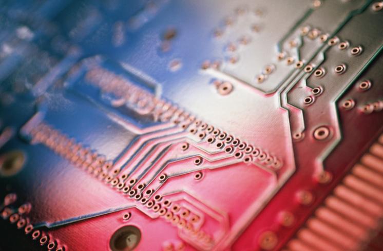
Trace Layout
Trace layout is another key component of reducing EMI in circuit boards. Traces are conductive paths that move flowing electrons within the circuit. Because traces conduct electrons, they present a high-risk for becoming antennas and radiating unwanted EMI.
- Avoid Right-Angles: Capacitance increases when traces exceed angles of 45 degrees. This may lead to reflection and EMI. Designing traces with rounded corners or angles of less than 45 degrees will help reduce the risk of EMI.
- Separate Signals: Separate high-speed and low-speed traces, as well as analog and digital signals.
- Shorten Return Paths: Return paths for signals should be as short as possible to minimize EMI.
- Pay Attention to Spacing: Traces that are too close together create crosstalk. Maintain a space of at least twice the trace width to prevent capacitive coupling.
- Be Careful with Vias: Vias allow you to use multiple board layers while routing your circuit, but sometimes add capacitance and inductance. This can lead to unwanted reflection between components.
Use EMI Shielding
In some cases, a certain amount of EMI is unavoidable. Luckily, it’s still possible to produce a high-quality circuit board by utilizing EMI shielding. Shielding is a protective layer, which prevents external EMI from effecting your component. External metal shields, like Faraday cages, are used to cover circuit boards to prevent nearby EMI from entering from neighboring sources. Some shields are also used to cover interior components to prevent EMI leaks within the board itself. Cables carry currents and are another risk factor for increased EMI. Fortunately, cables but can be shielded with a protective coating that reduces EMI and insulates high-frequency signals.
Work with a Trusted Manufacturer
One of the best ways to avoid EMI is to partner with a trusted PCB manufacturer. At Imagineering, we specialized in rigid and flexible circuit boards designed to meet your unique needs and specifications. Whether you’re looking for a prototype or seeking a more complex production run, the team at Imagineering is dedicated to providing high-quality results.
But with so many manufacturers in the market, why choose Imagineering?
- Quality: We are dedicated to providing aerospace quality components built to last. Choose from a wide selection of materials and finishes to achieve your ideal design.
- Price: We manufacture high-quality PCBs at prices you can afford. Our network of international manufacturers and our global buying influence allows us to offer first-class components that fit into any budget.
- Timing: Partnering with a PCB manufacturer shouldn’t mean delaying your project for months on end. Imagineering offers same-day turnaround for prototyping and low-volume production in 5-6 days, so you never have to put your ideas on hold.
- Simplicity: Managing multiple supply chains and navigating language barriers is exhausting and time-consuming. Imagineering is your one-stop-shop for PCBs from fabrication, to assembly, to delivery.
- Reliability: We adhere to industry standards to ensure our boards are functional, safe, and reliable. Among others, Imagineering is AS9100D/ISO9001:2015 Certified, RoHS certified, and an IPC member.
With our expertise, commitment to client satisfaction, and customer-friendly prices, it’s no wonder that Imagineering remains an industry leader in PCB manufacturing. Contact us today to get your initial quote.