
The printed circuit board, or PCB, is the foundational component of nearly every device we use on a daily basis, including phones, tablets, and computers.
However, despite being used in nearly every major consumer electronic, they suffer from one major weakness: sustainability.
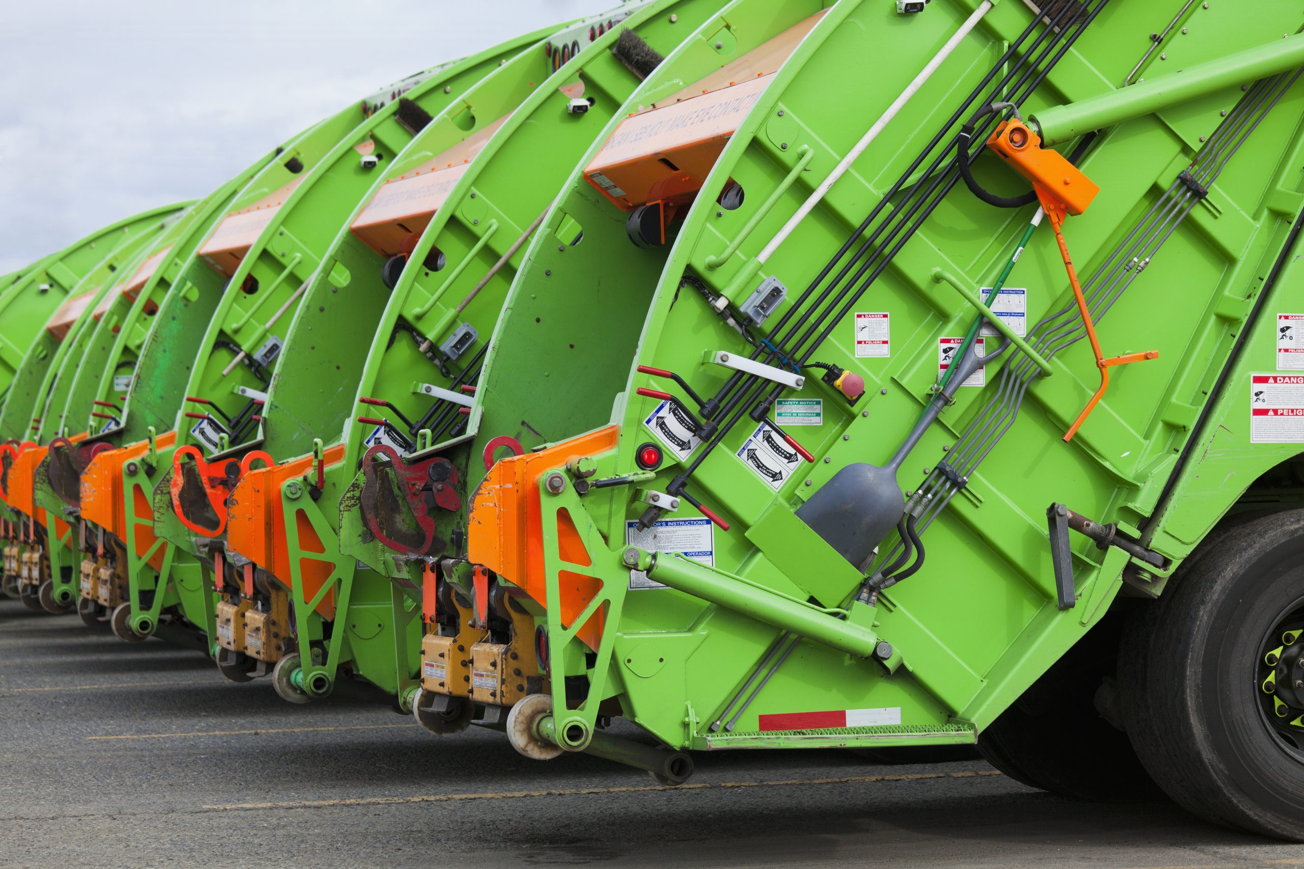
Traditional PCBs are not easily reused and can even be challenging to dispose of in an environmentally friendly way. These issues mean that PCBs are a major contributor to the global problem of electronic waste (also known as e-waste).
That problem may be on the verge of being solved.
Earlier this year, Infineon, a major producer of IoT technologies, announced that it would begin using Soluboard in its evaluation boards. Soluboard is a revolutionary new PCB substrate material that is dissolvable in water. This property will be easier to dispose of and can even lead to reusing electronic components recovered from old boards.
We’ve authored today’s blog to help catch you up on the current state of soluble PCBs, how they work, and the future of this exciting new material.
What are Traditional PCBs?
PCBs provide a compact and organized way to interconnect electrical components like microprocessors, capacitors, and integrated circuits. You can think of them as the foundation of the electronic circuit necessary to power a device and execute its functions.
The Basics of PCB Manufacturing
Here’s a quick overview of the traditional manufacturing process to give you an idea of how the technology is produced.
- The software designs PCBs, shapes, layouts, and components.
- Multiple layers of substrate material, traditionally fiberglass-reinforced epoxy resin (FR4), are bonded together with copper foil in between.
- Using a process known as photolithography, copper circuits are etched into the surface of the substrate, allowing for the precise formation of the conductive pathways that connect the electronic components of the PCB.
- Components are then soldered onto the PCB using a technique such as surface mount technology (SMT) or through-hole technology (THT).
The Limitations of Traditional PCBs
The printed circuit board is versatility makes it a staple in most technology. However, there are some clear drawbacks to the process of manufacturing PCBs that lead to widespread problems, especially with regard to their disposal.
- Waste: The manufacturing process can generate significant waste, including chemical byproducts and cut-off substrate material.
- Disposal: Due to their complex composition, disposal can often release harmful pollutants into the soil or atmosphere.
- Non-Biodegradable: Traditional PCBs are not biodegradable, which can lead to long-lasting environmental impacts.
Water Soluble PCBs: A Sustainable Alternative
To solve some of the problems traditional PCBs face with regards to waste management, researchers have been looking for ways to improve the manufacturing process using PCBs that dissolve in water.
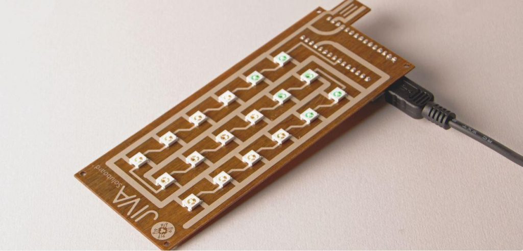
Promising solutions such as Soluboard, a flax-fiber-based composite material developed by Jiva Materials now exist.
In 2022, researchers from the University of Washington published this paper detailing a process they used to produce a mouse using Soluboard. As the researchers show, using functional, biodegradable PCBs to produce useful technology is now possible.
Traditional vs. Water Soluble Printed Circuit Boards
Here are three major differences that separate traditional and water-soluble printed circuit boards:
- Biodegradability: Soluboard is formulated to dissolve when exposed to boiling water. This is a fundamental departure from traditional PCBs, usually made from durable, long-lasting materials like FR4.
- Disposal Method: Traditional PCBs are usually disposed of by throwing them in a landfill or incinerating them. They can be recycled, but these methods are complex and energy-intensive. Soluble PCBs can easily be dissolved, and their components are recovered through simple filtering.
- Sustainability: Traditional PCBs are major contributors to the global problem of e-waste. Soluble PCBs promise to mitigate this with a design focused on renewability.
Overall, the development of Soluboard and similar materials reflects a broader commitment to responsible product life cycles worldwide.
3 Advantages of Water-Soluble Printed Circuit Boards
Soluble PCBs have 3 major advantages over traditional PCBs:
1. Reduced Environmental Impact
With a design focused on biodegradability, soluble boards promise to be easier to dispose of in an environmentally friendly way.
2. Component Reusability
The dissolution process of soluble boards allows for easier recovery of electronic components. This allows for more efficient use of resources and longer lifecycles for materials.
3. Broader Sustainability in Electronics
Incorporating biodegradable materials and sustainable design practices means that PCB makers can contribute directly to the global effort to make electronics production and disposal more sustainable.
What Makes Water-Soluble PCBs Possible?
Jiva Materials is a company founded in 2017 that sought to solve a fundamental problem of PCBs: the traditional material used, FR4, is not biodegradable and not easily recycled. This made PCBs a major contributor to the 50 million tons of e-waste produced each year worldwide.
Their solution, Soluboard, is a composite material primarily made from flax fiber. Flax fibers are natural, renewable, and dissolve in water, making them a more sustainable alternative to FR4.
How are Water Soluble PCBs Manufactured?
The design process of soluble PCBs is similar to traditional PCBs. It goes like this:
- Circuit boards are designed with standard software, just like traditional PCBs.
- Soluboards are then cut to desired shapes using techniques like laser cutting.
- Circuit traces are patterned onto the substrate using conductive ink.
- Next, components are carefully soldered onto the substrate forming a functional circuit.
- Finally, the board is encased in a 3D printed case of environmentally friendly materials such as polyvinyl alcohol (PVA) or compostable polylactic acid (PLA) filaments.
At the end of the device’s lifecycle, the flax fiber-based composite substrate can be dissolved, leaving behind electronic components that can be recycled.
What Impact Might Soluble PCBs Have?
Since soluble PCBs function the same way traditional PCBs do, they could be applied in a wide range of industries and products, including:
- Consumer Electronics, where companies who produce devices like smartphones and tablets can benefit from the simplified end-of-life recycling of valuable components.
- IoT and Smart Homes, where devices like thermostats, security cameras, and lights can adopt soluble PCBs that align with the eco-conscious lifestyle of modern consumers.
- Prototyping, where soluble PCBs can be used to produce prototypes that can easily be scrapped and renewed later, leading to greater efficiency in the design and testing process.
Impacts on All Major Industries
Water soluble PCBs have the potential to transform industries by providing a sustainable alternative to traditional electronic components. If they are widely used, we can expect massive impacts in:
- Environmental Sustainability: Improved end-of-life reusability will significantly reduce waste caused by less efficient PCB materials.
- Resource Efficiency: Reusability also means resource efficiency. Conserving valuable resources is not only better for the environment but may also reduce the cost of production.
- Innovation: Soluble PCBs may serve as an important touchstone in the philosophy of electronic designs and materials science, fostering a permanent shift towards more responsible technology development.
Challenges and Considerations for Water Soluble PCBs
We know that soluble PCBs are not only possible but in production today thanks to the work of companies like Jiva and Infineon. However, certain challenges must be overcome before we can expect widespread use of the technology.
Some of these challenges might include:
- Scaling to efficient, large-scale manufacturing with cost-effective methods while ensuring consistently high-quality output.
- Standardizing the process of manufacturing Soluboards across different production facilities.
- Ensuring that Soluboard-based devices remain cost-competitive with traditional electronics. Without this, market adoption will be an uphill battle.
Current Developments and Future Outlook for Soluble PCBs
Here’s the 60-second rundown of what you need to know about the current state of soluble PCB production and the near-term developments that we might expect from further research.
- Companies like Jiva Materials and Infineon have successfully developed soluble PCBs using flax-fiber-based composite material and conductive ink printing techniques.
- These boards can be dissolved in water to retrieve components and enable reusability.
- Increased reusability promises to reduce the carbon footprint associated with traditional PCB production.
The Near Future for Water Soluble PCBs
More optimization can be expected as this technology becomes more well-known and widely used.
Look for changes and improvements in:
- Material Refinement: Researchers may use this starting point to uncover improved biodegradable materials with even better properties.
- Component Reusability: Techniques for effectively reusing components may become standardized.
- Commercial Viability: As processes for production and reusability become more optimized, the commercial viability of soluble PCBs will increase.
- Regulatory Considerations: Finally, as the environmental impact of e-waste gains attention, regulatory agencies may enforce standards for sustainable electronics. If so, expect the state of soluble PCBs to play a crucial role in developing technologies.
The potential for soluble PCBs to revolutionize the electronics industry is exciting. By focusing research on biodegradable and sustainable materials, companies like Infineon and Jiva provide a pathway for tech companies worldwide to reduce their contribution to e-waste.
In the immediate future, there will still be challenges to the large-scale manufacture of these boards, and it may be months or even years before we start to see the first major products that use these materials.
Work with Imagineering the Certified Experts in PCBs
Imagineering’s PCB expertise gives you the highest quality printed circuit boards you need and the quick turnaround time you demand.
We are ITAR Registered, AS9100D/ISO 9001:2015 Certified, SAM Registered, RoHS Compliant, and an IPC Member.
The biggest brands in the world choose Imagineering for their printed circuit board fabrication and assembly; choose us, and you will see the difference.
We stay current with the latest advancements in all things related to printed circuit boards. Subscribe to our newsletter to stay up to date with our latest blogs!