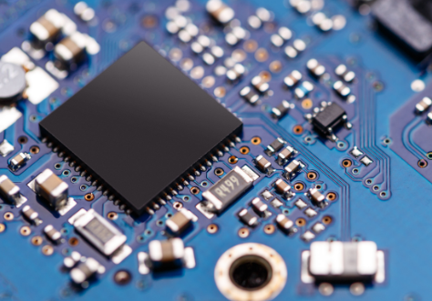
Simple printed circuit boards should function with little influence on other devices. As designs operate at higher speeds and are built on increasingly smaller boards, these factors become more difficult to mitigate. High-speed PCB design is the specialized field of creating boards that operate at peak functionality without interfering with its own signals, or the signals of other electronic devices nearby.
Ideally, a printed circuit board will have no signal distortion, can handle electromagnetic interference from nearby devices, and does not generate significant interference of its own. High-speed PCB design refers to any printed circuit board design where the physical characteristics of a board start to alter the signals being sent through the board itself. Issues like delays, crosstalk, attenuation, and reflections may occur when interference is significant. While a simple board will likely not produce these kinds of issues, the proliferation of more complex boards poses a threat to operationality.
What causes issues in high-speed PCB design, and what can designers and manufacturers do to reduce these problems? In this blog, we outline everything you need to know about this burgeoning field of printed circuit board troubleshooting.
What is Signal Integrity in PCB?
Signal integrity is a printed circuit boards’ ability to deliver signals without distortion. It refers to the quality of the signals that pass through a transmission line. As manufacturers push printed circuit boards to operate at increasingly higher speeds, they become susceptible to signal integrity problems. While all printed circuit boards are subject to issues of signal integrity, it doesn’t become a concern until PCBs operate at speeds greater than 50MHz.
Signal integrity issues occur when:
- The shape of a signal changes from the intended state.
- Electrical noise degrades the signal to noise ratio
- Undesired noise influences other signals and circuits on a PCB.
When signal integrity issues begin to appear in a printed circuit board, it may not work optimally. More concerning, signal integrity issues may not appear in the prototype stage, but will show up later on or in different production lots.
Thus, the best high-speed PCB design must not only focus on creating ultrafast, high-performing boards, but boards that don’t hamper their own performance.
How to Prevent Signal Integrity Issues in High-Speed PCB Design?
High-speed printed circuit board design has become a focus of the field at large. As boards become more complex, more research is being conducted into how to mitigate signal integrity issues while creating smaller and faster boards. While entire research papers are dedicated to the subject, we have compiled several suggestions for preventing signal integrity issues in high-speed PCB design:
Design Around Your Stackup – Signal integrity can be controlled by clearly defining ground and keeping ground near important traces during routing. By alternating between signal, power, and ground layers, a design can leverage shielding, low-impedance return, and control over impedance lines.
Control Line Impedance – The quality of a signal is determined by the trace on a printed circuit board. If the impedance of a trace line isn’t uniform, signal distortion will occur. This can be prevented by utilizing consistent spacing and length matching for differential pairs.
Identify Signal Integrity Issues in Simulations – Simulating a printed circuit board’s functionality is essential during the design process, as it can help indicate potential issues before they are sent off to a printed circuit board manufacturer. Ideally, this step is taken even before a prototype is created.
Signal Integrity Testing – Several tests exist to determine signal integrity, but for digital designs using a vector network analyzer as well as eye diagram tests can help identify issues well in advance before manufacturing occurs.
In summary, two takeaways of high-speed PCB design can be summarized as conducting simulations to ensure the design is ideal, and not starting fabrication and assembly until after all the boxes have been checked. Failing to do the proper work to limit signal interference is expensive, takes up time, and in a worst-case scenario, can provide your end-user with a faulty product.
High-Speed PCBs at Imagineering
As printed circuit boards grow more complex, you need a printed circuit board manufacturer that is up to the task to create flawless PCBs delivered on time. Trust Imagineering. With Class 3 Certification and on-time delivery guaranteed, we have proven to be a valuable asset in a changing world of printed circuit board design. Contact us today for more information about our services, or request a quote here.

